SANYO 2SJ263 handbook
Contents
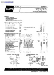
1. 253263 _ P Channel MOS Silicon FET Very High Speed Switching Applications Features Low ON resistance Very high speed switching Low voltage drive Micaless package facilitating mounting Absolute Maximum Ratings at Ta 25 C unit Drain to Source Voltage Voss 60 V Gate to Source Voltage Vass 15 V Drain Current DC Ip A Drain Current Pulse Ipp PW 10zs duty cycle 1 24 A Allowable Power Dissipation Pp 20 W T 25 C 25 W Channel Temperature Tch 150 C Storage Temperature Tstg 5 to 150 C Electrical Characteristics at Ta 25 C min typ max unit D S Breakdown Voltage Vempss Ip 1mA Vgs 0 60 V _ G 5 Breakdown Voltage Vermncss Ig 1002A Vps 0 15 V Zero Gate Voltage Ipss Vps 60V Vgs 0 100 p Drain Current Gate to Source Leakage Current less Vos 12V Vps 0 10 pA Cutoff Voltage Vesom Vps 10V Ip ImA 1 0 2 0 V Forward Transfer Admittance Ysl Vps 10V Ip 4A 3 5 6 S Static Drain to Source RDSon Ip 4A Vgs 10V 150 200 mf on State Resistance RDSon Ip 4A Vgs 4V 200 270 mQ Input Capacitance Ciss Vps 20V f 1MHz 950 pF Output Capacitance Coss Vps 20V f 1MHz 300 pF Reverse Transfer Capacitance C ss Vps 20V f 1MHz 75 pF Turn ON Delay Time td on See specified Test Circuit 15 ns Rise Time tr 4 45 ns Turn OFF Delay Time ta off 90 ns Fali Time tf Z 110 ns Diode Forward Voltage Vsp Is 6A Vgs 0 1 0 1 5 Vv Switch2. implants life support systems aerospace equipment nuclear power control systems vehicles disaster crime prevention equipment and the like the failure of which may directly or indirectly cause injury death or property loss W Anyone purchasing any products described or contained herein for an above mentioned use shall Accept full responsibility and indemnify and defend SANYO ELECTRIC CO LTD its affiliates subsidiaries and distributors and all their officers and employees jointly and severally against any and all claims and litigation and all damages cost and expenses associated with such use Not impose any responsibility for any fault or negligence which may be cited in any such claim or litigation on SANYO ELECTRIC CO LTD its affiliates subsidiaries and distributors or any of their officers and employees jointly or severally Information including circuit diagrams and circuit parameters herein is for example only it is not guarant eed for volume production SANYO believes information herein is accurate and reliable but no guarantees are made or implied regarding its use or any infringements of intellectual property rights or other rights of third parties No 4234 3 3
3. ing Time Test Circuit Package Dimensions 2063 E Yop 30v unit mm z4 sov U Ipe 4A Vin AL 7 50 Bi oa vour gt c 3 P G S Source ae ies D Drain G Gate SANYO TO 220ML SANYO Electric Co Ltd Semiconductor Business Headquarters TOKYO OFFICE Tokyo Bldg 1 10 1 Chome Ueno Taito ku TOKYO 110 JAPAN 42893TH KOTO AX 8376 No 4234 1 3 Drain Current Ip A Forward Transfer Admittance Y S on State Resistance Rogon 2 Static Drain to Source Switching Time SW Time ns o 25J263 O Drain to Source Voltage V pg V TT Ip Drain Current Ip A Ros on Te Case Temperature T C SWTime Ip 1 0 Drain Current Ip A Static Drain te Source Drain Current Ip A Gate to Source Voltage Vgs V Rps on VGs T 25 C G 0 G AUV a d z 3 T vi z 3 3 a 2 2 8 10 12 14 16 Gate to an Voltage Vgs V ssr Crss Vos 5 oy zn 2 D 35 8 O 0 4 12 16 20 24 28 32 Drain to Source Voltage Vps V 5 ASO e LHE a T sAN RADSIN i A ah a i E 1 cy Drain to Sourc Voltage Vps V No 4234 2 3 Allowable Power Dissipation Pp W 285263 Allowable Power Dissipation Pp W Ambient Temperature T C Case Temperature T C W No products described or contained herein are intended for use in surgical
Download Pdf Manuals

Related Search
SANYO 2SJ263 handbook