FAIRCHILD FDD8445 Manual
Contents
1. t RECTANGULAR PULSE DURATION s Figure 4 Peak Current Capability 1 2 80 r m Vgs710V u CURRENT LIMITED a 10 BY PACKAGE E d 60 208 E zZ E a lt 0 6 2 40 z d a 04 x ir 620 0 2 n 0 0 0 0 25 50 75 100 125 150 175 25 50 75 100 125 150 175 Tc CASE TEMPERATURE C Tc CASE TEMPERATURE C Figure 1 Normalized Power Dissipation vs Case Figure 2 Maximum Continuous Drain Current vs Temperature Case Temperature 2 T ina FEFE Fa seat DUTY CYCLE DESCENDING ORDER 1 z o Y m2 D 0 50 UN 0 20 Pom EA FT o1 H 92 0 05 W N 01 0 02 D t du oo t a L z NOTES o DUTY FACTOR D t t 2 PEAK T Poy X Zgyc X Rose Tc SINGLE PULSE pene eee HL ELLII 10 10 10 10 10 10 10 t RECTANGULAR PULSE DURATION s Figure 3 Normalized Maximum Transient Thermal Impedance 2000 T T TTTTTT T T T TT T Theale Ves 7 10V TRANSCONDUCTANCE Tc 25 C 1000 lt lt MAY LIMIT CURRENT FOR TEMPERATURES 4 T IN THIS REGION ABOVE 25 C DERATE PEAK H CURRENT AS FOLLOWS T Z Z al g l bs i 5 150 o x 100 ul n 2 2 SINGLE PULSE 10 Ce Ea TE 10 10 10 10 102. No Identification Needed Full Production This datasheet contains final specifications Fairchild Semiconductor reserves the right to make changes at any time without notice to improve design Obsolete Not In Production This datasheet contains specifications on a product that has been discontinued by Fairchild Semiconductor The datasheet is printed for reference information only Rev 124 FDD8445 Rev A W 7 www fairchildsemi com LAASOW q U9Uue1J 119 Mog Jouueu N SppSada
3. 1 9 C W RoJA Thermal Resistance Junction to Ambient TO 252 lin copper pad area 52 9CAN Package Marking and Ordering Information Device Marking Device Package Reel Size Tape Width Quantity FDD8445 FDD8445 TO 252AA 13 12mm 2500 units Electrical Characteristics 1 25 C unless otherwise noted Symbol Parameter Test Conditions Min Typ Max Units Off Characteristics BVpss Drain to Source Breakdown Voltage Ip 250uA Veg OV 40 V Vps 32V 2 i 1 pA l Zero Gate Voltage Drain Current DS DSS 3 Vas 0V Tj 150 C 250 lass Gate to Source Leakage Current Vas 20V 2 100 nA On Characteristics Vesith Gate to Source Threshold Voltage Vps Ves lp 250A 2 2 8 4 V Ip 50A Vas 10V 6 7 8 7 R i i DS ON Drain to Source On Resistance Ip 50A Veg 10V 125 163 mQ Ty 175 C Dynamic Characteristics Ciss Input Capacitance E 3040 4050 pF Vps 25V Veg OV Coss Output Capacitance f 1MHz E 295 390 pF Crss Reverse Transfer Capacitance 178 270 pF Re Gate Resistance f 1MHz 1 7 Q Qgrror Total Gate Charge at 10V Veg 0 to 10V 45 59 nC Qgs Total Gate Charge at 5V Ves 0 to 5V 17 22 nC Qg TH Threshold Gate Charge Veg 0102V Vpp 20V 5 8 7 6 nC Qgs Gate to Source Gate Charge Ip 50A 12 5 nc Qgs2 Gate Charge Threshold to Plateau 9 5 z nC Qya Gate to Drain Miller Charge 10 5 nC FDD8445 Rev A W 2 www fairchildsemi com LAASOW q U9Uue1J 1o Mog Jouueu N SppSada Electrical Characteristic
4. 10 10 FDD8445 Rev A W 4 www fairchildsemi com LAASOW q U9Ue1J11oMog JeUULYD N SppSada Typical Characteristics 1000 10us pu C100 5 100us y 2 5 10 o z x q CURRENT LIMITED 1ms E 1 BY PACKAGE x Ff areamayee SNGLEPULSE A Ty MAX RATED ms LIMITED BY roston 25 C B 0 1 1 10 100 V DRAIN SOURCE VOLTAGE V Ds Figure 5 Forward Bias Safe Operating Area 140 PULSE DURATION 80ys DUTY CYCLE 0 5 MAX 120 Ip DRAIN CURRENT A 20 25 30 35 40 45 50 55 6 0 Ves GATE TO SOURCE VOLTAGE V Figure 7 Transfer Characteristics 20 PULSE DURATION 80uS 12A p DUTY CYCLE 0 5 MAX R GQ 16 W o E E12 o 7 W y Zz 8 o Rps ou DRAIN TO SOURCE 3 5 4 5 6 0 7 5 9 0 10 Vas GATE TO SOURCE VOLTAGE V Figure 9 Drain to Source On Resistance Variation vs Gate to Source Voltage N e e IfR 0 tav L Iag 1 3 RATED BVpss Vpp IfRz0O tav L R In las R 1 3 RATED BVpss Vpp 1 e e STARTING T 25 C e las AVALANCHE CURRENT A 0 01 0 1 1 10 100 tav TIME IN AVALANCHE ms 1000 NOTE Refer to Fairchild Application Notes AN7514 and AN7515 Figure 6 Unclamped Indutive Switching Capabili
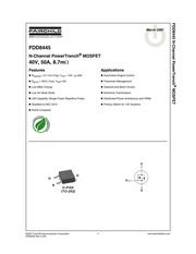
5. A FAIRCHILD March 2007 HERPES SEMICONDUCTOR FDD8445 N Channel PowerTrench MOSFET 40V 50A 8 7mQ Features Applications E Hps ow 6 7 mQ Typ Vas 10V Ip 50A W Automotive Engine Control E Qg 10 45nC Typ Vas 10V W Powertrain Management m Low Miller Charge W Solenoid and Motor Drivers W Low Qrr Body Diode W Electronic Transmission W UIS Capability Single Pulse Repetitive Pulse W Distributed Power Architecture and VRMs m Qualified to AEC Q101 W Primary Switch for 12V Systems W RoHS Compliant ERE E Eh a z T zZ FS S D PAK TO 252 2007 Fairchild Semiconductor Corporation 1 www fairchildsemi com FDD8445 Rev A W LAASOW q U9Uue1L11o9Mog Jouueu N SppSada Absolute Maximum Ratings T 25 C unless otherwise noted Symbol Parameter Ratings Units Voss Drain to Source Voltage 40 V Vas Gate to Source Voltage 20 V Drain Current Continuous Vgs 10v Note 1 70 A Ip Continuous Vgg 10v with Roya 52 C W 15 2 A Pulsed Figure 4 Eas Single Pulse Avalanche Energy Note 2 144 mJ p Power Dissipation 79 Ww 3 Derate above 25 C 0 53 W C Ty Tera Operating and Storage Temperature 55 to 4175 C Thermal Characteristics Roc Thermal Resistance Junction to Case
6. ESE SPECIFICATIONS DO NOT EXPAND THE TERMS OF FAIRCHILD S WORLDWIDE TERMS AND CONDITIONS SPECIFICALLY THE WARRANTY THEREIN WHICH COVERS THESE PRODUCTS LIFE SUPPORT POLICY FAIRCHILD S PRODUCTS ARE NOT AUTHORIZED FOR USE AS CRITICAL COMPONENTS IN LIFE SUPPORT DEVICES OR SYSTEMS WITHOUT THE EXPRESS WRITTEN APPROVAL OF FAIRCHILD SEMICONDUCTOR CORPORATION As used herein 1 Life support devices or systems are devices or systems 2 A critical component in any component of a life support which al dia intended for surgical implant into the body or device or system whose failure to perform can be b support or sustain life and c whose failure to perform reasonably expected to cause the failure of the life support when properly used in accordance with instructions for use device or system or to affect its safety or effectiveness provided in the labeling can be reasonably expected to result in a significant injury of the user PRODUCT STATUS DEFINITIONS Definition of Terms Datasheet Identification Product Status Definition Advance Information Formative or In Design This datasheet contains the design specifications for product develo ment Specifications may change in any manner without notice Preliminary First Production This datasheet contains preliminary data supplementary data will be published at a later date Fairchild Semiconductor reserves the right to make changes at any time without notice to improve design
7. following are registered and unregistered trademarks Fairchild Semiconductor owns or is authorized to use and is not intended to be an exhaustive list of all such trademarks ACEx HiSeC Programmable Active Droop TinyLogic Across the board Around the world i Lo QFET TINYOPTO ActiveArray ImpliedDisconnect Qs TinyPower Bottomless IntelliMAX QT Optoelectronics TinyWire Build it Now ISOPLANAR Quiet Series TruTranslation CoolFET MICROCOUPLER RapidConfigure uSerDes CROSSVOLT MicroPak RapidConnect UHC CTL MICROWIRE ScalarPump UniFET Current Transfer Logic MSX SMART START VCX M DOME MSXPro SPM Wire E CMOS ocx STEALTH EcoSPARK OCXPro SuperFET EnSigna OPTOLOGIC SuperSOT 3 FACT Quiet Series OPTOPLANAR SuperSOT 6 FACT PACMAN SuperSOT 8 FAST POP SyncFET FASTr Power220 TCM FPS Power247 The Power Franchise FRFET PowerEdge TM GlobalOptoisolator PowerSaver TinyBoost GTO PowerTrench TinyBuck DISCLAIMER FAIRCHILD SEMICONDUCTOR RESERVES THE RIGHT TO MAKE CHANGES WITHOUT FURTHER NOTICE TO ANY PRODUCTS HEREIN TO IMPROVE RELIABILITY FUNCTION OR DESIGN FAIRCHILD DOES NOT ASSUME ANY LIABILITY ARISING OUT OF THE APPLICATION OR USE OF ANY PRODUCT OR CIRCUIT DESCRIBED HEREIN NEITHER DOES IT CONVEY ANY LICENSE UNDER ITS PATENT RIGHTS NOR THE RIGHTS OF OTHERS TH
8. s 1 25 c unless otherwise noted 1 Maximum package current capability is 50A 2 Starting Ty 25 C L 0 18mH l4s 40A Symbol Parameter Test Conditions Min Typ Max Units Switching Characteristics tion Turn On Time z z 138 ns ta on Turn On Delay Time 10 ns t Turn On Rise Time Vpp 20V Ip 50A 82 ns la otf Turn Off Delay Time Ves 10V Reg 20 26 ns t Turn Off Fall Time 9 6 ns lor Turn Off Time 53 ns Drain Source Diode Characteristics Igp 50A 1 25 V Vsp Source to Drain Diode Voltage SD Isp 25A 1 0 V trr Reverse Recovery Time Ip 50A dlp dt 100A us 39 ns Qe Reverse Recovery Charge Ip 50A dlg dt 100A us 38 nC Notes This product has been designed to meet the extreme test conditions and environment demanded by the automotive industry For a copy of the requirements see AEC Q101 at http www aecouncil com All Fairchild Semiconductor products are manufactured assembled and tested under ISO9000 and QS9000 quality systems certification FDD8445 Rev A W www fairchildsemi com LAASOW q U9Uue1J11oMog Jouueu N SppSada Typical Characteristics
9. ty e eo e Ip DRAIN CURRENT A a o 20 0 0 0 5 1 0 1 5 2 0 2 5 3 0 Vps DRAIN TO SOURCE VOLTAGE V Figure 8 Saturation Characteristics T T T PULSE DURATION 80 S DUTY CYCLE 0 5 MAX NORMALIZED DRAIN TO SOURCE ON RESISTANCE 120 T JUNCTION TEMPERATURE C Figure 10 Normalized Drain to Source On Resistance vs Junction Temperature FDD8445 Rev A W www fairchildsemi com LAASOW q U9Uue1J11oMog Jouueu N SppSada Typical Characteristics 1 2 e e e e NORMALIZED GATE THRESHOLD VOLTAGE zi 40 0 40 80 120 T JUNCTION TEMPERATURE C 160 200 Figure 11 Normalized Gate Threshold Voltage vs Junction Temperature Ciss 1000 CAPACITANCE pF 100 0 1 1 10 Vps DRAIN TO SOURCE VOLTAGE V 40 Figure 13 Capacitance vs Drain to Source Voltage NORMALIZED DRAIN TO SOURCE BREAKDOWN VOLTAGE Breakdown Voltage vs Junction Temperature eo Ves GATE TO SOURCE VOLTAGE V 40 0 40 80 120 160 T JUNCTION TEMPERATURE C 200 Figure 12 Normalized Drain to Source 0 20 40 Q GATE CHARGE nC 60 Figure 14 Gate Charge vs Gate to Source Voltage FDD8445 Rev A W www fairchildsemi com LAASOW q U9Uue1J11oMog Jouueu N SppSada ea FAIRCHILD jee SEMICONDUCTOR TRADEMARKS The
Download Pdf Manuals

Related Search
FAIRCHILD FDD8445 Manual