mosaic PUMA68S4000X - 010/012/015/017 handbook
Contents
1. Voltage on any pin relative to Vss Power Dissipation Pr Storage Temperature Tste 55 DC Output Current Notes 1 Stresses above those listed may cause permanent damage to the device This is a stress rating only and functional operation of the device at these or any other conditions above those indicated in the operational sections of this specification is not implied Exposure to absolute maximum rating conditions for extended periods may affect reliability Recommended Operating Conditions Parameter Symbol Supply Voltage Voc 4 5 5 0 5 5 V Input High Voltage Vin 2 2 Vcc 0 3 V Input Low Voltage vi 0 3 0 8 V Operating Temperature Commercial Ta 0 70 c Industrial Ta 40 85 G I Suffix Notes 1 Pulse Width 3 0V for less than 5ns DC Electrical Characteristics V 5V 10 T 40 C to 85 C Parameter Test Condition Input Leakage Current lu Vin 0V to Vcc 20 20 uA Output Leakage Current ILo Vvo 0V to Vcc 20 20 uA Operating Supply Current 32 Bit Iccg2_ CS Vit lvo 0mA f fmax 750 mA 16 Bit Icc s CS Vu lvo 0mA f fmax 490 mA 8Bit Iccs CS Vi lvo 0mA f fuax 370 mA Standby Supply Current TTL Isp aw 2 250 mA Output Voltage Low Vor loL 8 0mA Vcc Min 0 4 V Output Voltage High Von lon 4 0mA Vcc Min 2 4 V Notes 1 CS1 4 inputs operate simultaneously for 32 bit2. Devices packaged in dry nitrogen JED STD 020 Packaged in trays as standard Tape and reel available for shipment quantities exceeding 200pcs upon request Soldering Recomendations IR Convection Ramp Rate 6 C sec max Temp exceeding 183 C 150 secs max Peak Temperature 225 C Time within 5 C of peak 20 secs max Ramp down 6 C sec max Vapour Phase Ramp up rate 6 C sec max Peak Temperature 215 219 C Time within 5 C of peak 60 secs max Ramp down 6 C sec max The above conditions must not be exceeded Note The above recomendations are based on standard industry practice Failiure to comply with the above recomendations invalidates product warranty PAGE 11 Issue 5 1 April 2001 2 S o 3 D e S S D 7
3. During Vcc power up a pull up resistor to Vcc on CS is required to meet SB specification 2 This parameter is sampled and not 100 tested 3 For test conditions see AC Test Conditions Figures A B C 4 tc z and toyz are specified with CL 5pF as in Figure C Transition is measured 500mV from steady state voltage 5 This parameter is guaranteed but not tested 6 WE is HIGH for read cycle 7 CS and OE are LOW for Read cycle 8 Address valid prior to or coincident with CS transition LOW 9 All read cycle timings are referenced from the last valid address to the first transitioning address 10 CS or WE must be HIGH during address transitions 11 All write cycle timings are referenced from the last valid address to the first transitioning address PAGE 8 Issue 5 1 April 2001 PUMA 68 pin JEDEC Surface Mounted PLCC N gt D Q O a 8 D LUAN UT CUO TTT O O CU QUUUUUUUEU ITT 25 27 0 995 25 02 0 985 E __ 1 27 0 050 23 11 0 910 24 13 0 950 PAGE 9 Issue 5 0 August 1999 Ordering Information PUMA 68S4000XLI 010 Note FL Speed Power Consumption Pinout Configuration Memory Organisation Technology Package 010 012 015 017 Temp Range Screening Blank Blank X 4000 S PUMA 68 10ns 12ns 15ns 17ns Commercial Industrial Standard Industry Standard Pinout configurable as 128
4. 7 ns Address Access Time taa 10 12 15 17 ns a Chip Select Access Time tacs 10 12 15 17 ns S Output Enable to Output Valid toe 5 6 7 8 ns Output Hold From Address Change toH 2 3 3 3 ns 2 Chip Selection to Output in Low Z tc z 3 3 3 3 ns Output Enable to Output in Low Z tolz 0 0 0 0 ns Chip Deselection to Output in High Z tcuz 0 5 0 6 0 8 0 9 ns Output Disable to Output in High Z touz 0 4 0 5 0 7 0 8 ns Write Cycle Parameter Symbol Min i i i Units Write Cycle Time 10 ns Chip Selection to End of Write 9 ns Address Valid to End of Write 9 ns Address Setup Time 0 ns Write Pulse Width 8 ns Write Recovery Time 0 ns Data to Write Time Overlap 6 ns Output Active from End of Write 0 ns Data Hold time from Write Time 0 ns Write to Output in High Z ns Under Development PAGE 5 Issue 5 1 April 2001 Read Cycle 1 367 9 Address Controlled Address Dour Data Valid Read Cycle 2 3 CS Controlled CS OE Dout Current Supply Notes 1 During Vcc power up a pull up resistor to Vcc on CS is required to meet SB specification 2 This parameter is sampled and not 100 tested 3 For test conditions see AC Test Conditions Figures A B C 4 tc z and tenz are specified with CL 5pF as in Figure C Transition is measured 500mV from steady state voltage 5 This parameter is guaranteed but not tested 6 WE is HI
5. GH for read cycle 7 CS and OE are LOW for Read cycle 8 Address valid prior to or coincident with CS transition LOW 9 All read cycle timings are referenced from the last valid address to the first transitioning address 10 CS or WE must be HIGH during address transitions 11 All write cycle timings are referenced from the last valid address to the first transitioning address PAGE 6 Issue 5 1 April 2001 3 3 Q 5 S S 3 17 Write Cycle 1 1 WE Controlled Address WE Dour Notes 1 During Vcc power up a pull up resistor to Vcc on CS is required to meet SB specification 2 This parameter is sampled and not 100 tested 3 For test conditions see AC Test Conditions Figures A B C 4 tc z and tenz are specified with CL 5pF as in Figure C Transition is measured 500mV from steady state voltage 5 This parameter is guaranteed but not tested 6 WE is HIGH for read cycle 7 ICS and OE are LOW for Read cycle 8 Address valid prior to or coincident with CS transition LOW 9 All read cycle timings are referenced from the last valid address to the first transitioning address 10 CS or WE must be HIGH during address transitions 11 All write cycle timings are referenced from the last valid address to the first transitioning address PAGE 7 Issue 5 1 April 2001 Write Cycle 2 1 CS Controlled tow gt CS tw WE ty gt tw gt 73 toH Din Data Valid Dour Notes 1
6. K x 8 256K x 16 or 512K x 8 SRAM 68 pin J Leaded PLCC Although this data is believed to be accurate the information contained herein is not intended to and does not create any warranty of merchantibility or fitness for a particular purpose Our products are subject to a constant process of development Data may be changed without notice Products are not authorised for use as critical components in life support devices without the express written approval of a company director PAGE 10 http www mosaicsemi com Issue 5 1 April 2001 P40 Una jeunoyu b 3 Visual Inspection Standard All devices inspected to ANSI J STD 001B Class 2 standard Moisture Sensitivity Devices are moisture sensitive Shelf Life in Sealed Bag 12 months at lt 40 C and lt 90 relative humidity RH After this bag has been opened devices that will be subjected to infrared reflow vapour phase reflow or equivalent processing peak package body temp 220 C must be A Mounted within 72 Hours at factory conditions of lt 30 C 60 RH OR B Stored at lt 20 RH If these conditions are not met or indicator card is gt 20 when read at 23 C 5 devices require baking as specified below If baking is required devices may be baked for A 24 hours at 125 C 5 for high temperature device containers OR B 192 hours at 40 C 5 C 0 C and lt 5 RH for low temperature device containers Packaging Standard
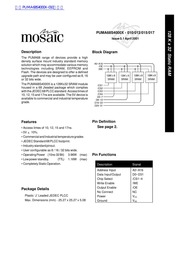
7. O0 O0 PUMA68S4000x 010 O O ba MOSalC The PUMA68 range of devices provide a high density surface mount industry standard memory solution which may accommodate various memory technologies including SRAM EEPROM and Flash The devices are designed to offer a defined upgrade path and may be user configured as 8 16 or 32 bits wide The PUMA68S4000X is a 128Kx32 SRAM module housed in a 68 Jleaded package which complies with the JEDEC 68 PLCC standard Access times of 10 12 15 and 17ns are available The 5V device is available to commercial and industrial temperature grade Features e Access times of 10 12 15 and 17ns e5V 10 e Commercial and Industrial temperature grades JEDEC Standard 68 PLCC footprint Industry standard pinout User configurable as 8 16 32 bits wide e Operating Power 10ns 32Bit 3 96W max e Low power standby TTL 1 16W max e Completely Static Operation Package Details Plastic J Leaded JEDEC PLCC Max Dimensions mm 25 27 x 25 27 x 5 08 PUMA68S4000X 010 012 015 017 Issue5 1 April 2001 Block Diagram 128K x 8 SRAM Pin Definition See page 2 Pin Functions Signal Description Address Input Data Input Output Chip Select Write Enable Output Enable No Connect Power Ground N amp EN x N o 2 O J D Pin Definition PUMA68S4000X PAGE 2 Issue 5 1 April 2001 Absolute Maximum Ratings Parameter
8. mode in pairs for 16 bit mode and singly for 8 bit mode 2 At f f ax address and data inputs are cycling at max frequency 3 All currents are specified for 10ns PAGE 3 Issue 5 1 April 2001 O Q S Q O Q S a Q S 17 Capacitance Voc 5 0V T 25 C F 1MHz Parameter Symbol Input Capacitance Address OE WE Cini Cio Output Capacitance 8 bit mode worst case Note These Parameters are calculated not measured Test Conditions Input pulse levels OV to 3 0V Input rise and fall times 3ns e Input and Output timing reference levels 1 5V e Output Load See Load Diagram e Vec 9V410 PUMA module tested in 32 bit mode Operation Truth Table CS1 CS2 CS3 CS4 r OE WE Supply Current Test Condition Min Typ Max Unit 30 pF 38 pF Output Load IO Pin 1662 1 76V 30pF Write DO D7 Write D8 D15 Write D16 D23 Write D24 D31 rm rm IIc I ar Write DO D15 locs Read D24 D31 lcc16 Read D0 D15 lcc16 Read D16 D31 Icca2 Read DO D31 lcc32 lcc16 lcc8 DO D31 High Z XJTITJTJITJTITJI lsg Isg DO D31 Standby Notes H V L V X V p or Va PAGE 4 Issue 5 1 April 2001 Read Cycle gt gt S Parameter Min Max Min Max Min Max Min Max Units Read Cycle Time tre 10 12 15 1
Download Pdf Manuals

Related Search
mosaic PUMA68S4000X 010/012/015/017 handbook