ST M28W640ECT M28W640ECB Manual
Contents
1. 13 2 55 M28W640ECT M28W640ECB Block Lock Down 13 Tabler4 Commands 2 AA AAA a et wp 14 Table 5 Read Electronic 14 Table 6 Read Block Lock 15 Table 7 Read Protection Register and Lock Register 15 Table 8 Program Erase Times and Program Erase Endurance Cycles 16 BLOCK LOCKING A 16 Locked SP OE ee eb ats 16 Unlocked Stat itinerario hi S 16 Lock Down State E RED 17 Reading a Block s Lock Status 16 Locking Operations During Erase Suspend 17 Table 9 Block Lock Status 17 Table 10 Protection 5 5 18 STATUS REGISTER 2000 AA EEG ME M ER dada 19 Program Erase Controller Status Bit 7 19 Erase Suspend Status 6 19 Eraserstatus Bite uy oL kd ep Dates did a 19 Program Status Bit Leere bela dod eee e e2. min Program Voltage Program or Erase operations gt 2 7V 5 VIL VoL 1 Program Voltage or Erase operations Program Voltage VPPLK Program and Erase lock out Vpp Supply Voltage Program and Erase lock out A lt O BB 23 55 M28W640ECT M28W640ECB Figure 9 Read AC Waveforms 000 0015 ADDR VALID gt 4 OUTPUTS pig DATA VALID STANDBY gt CHIP ENABLE ENABLED Al04387 Table 16 Read AC Characteristics Parameter Jr ow ww os mnnera we EEE e we o e ee o peteretur e ECC Output Enable Low to Output Transition Min Note 1 Sampled only not 100 tested 2 G may be delayed by up to teLav after the falling edge of E without increasing teLav 3 To be characterized 24 55 28 640 28 640 Figure 10 Write Waveforms Write Enable Controlled 888r0lV ONITIOd 151 lt 83 1S 038 01918 gt WHISNOO 90 135 dd N A MANO HMHdMi
3. E ME NERONE QE de fa 10 Output Disable bees rr AAA P 10 10 Automatic Stangaby 10 exerted od da a ie 10 Read Electronic Signature 11 Table 2 B s Operations sic v c es eed ag 10 COMMAND INTERFACE 2 mx aw m oe 11 Read Memory Array 1 1 11 Read Status Register 11 Read Electronic Signature 11 Table 3 Command 11 Read CFI Query 11 Block Erase Command ee Rr Mee BR bee ee 11 Program Commander aaa ace aides 12 Double Word Program 12 Clear Status Register 12 Program Erase Suspend Command 12 Program Erase Resume Command 13 Protection Register Program Command
4. TaM O V LVG HO ONVININOO 145 4 h 2 salsio38 SNLYLSY viva 10 ano GNVWWOO H3AQ gt SES 39V83 HO gt 27 55 28 640 28 640 Table 18 Write AC Characteristics Chip Enable Controlled Symbol Parameter tos Data Valid to Data Valid to Chip Enable High Enable High Min ea Enable High to Address 2 Transition ton Chip Enable High to Data Transition Enable High to Data Transition Min E Enable High to Chip Enable Low Chip Enable High to Write Enable High Chip Enable High to Write Enable High High to Write Enable High Min Min Papa jeje MOMIA an p AO pu e mper Note 1 Sampled only not 10095 tested 2 Applicable if is seen as a logic input lt 3 6V 3 To be characterized 28 55 M28W640ECT M28W640ECB Figure 12 Power Up and Reset AC Waveforms tVDHPH VDD VDDQ Power Up 1035376 Table 19 Power Up and Reset AC Characteristics Parameter Test Condition During Program Enable Low Output Enable Low mm others Min 30 0 Note
5. ua1sioau snivis ONVININOO HMAC gt HMIM HMAV 0 25 55 28 640 28 640 Table 17 Write Characteristics Write Enable Controlled gt FP past A ee EAS EEE pc Tea n d tos Chip Enable Low to Write Enable Low Chip Enable Low to Write Enable Low _ Enable Low to Write Enable Low o ns El APS E fw fe towel ER E IE Output Valid to Write ProtectLow Valid to Write Protect Low Min ES ee tit fa se O II MOE we a 9 r wes O io cn atotow 9 ve wiece non ws o m v Dew m Note 1 Sampled only not 100 tested 2 Applicable if is seen as a logic input lt 3 6V 3 To be characterized 26 55 M28W640ECT M28W640ECB Figure 11 Write AC Waveforms Chip Enable Controlled 68 01 SNIT1Od 15 qvaqd 95345934 SNLVLS WHIHNOO
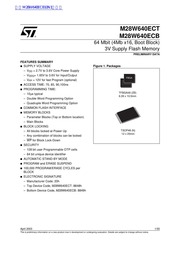
6. M28W640ECBION1 57 FEATURES SUMMARY m SUPPLY VOLTAGE Vpp 2 7 to 3 61 Core Power Supply 1 65V to for Input Output Vpp 12V for fast Program optional m ACCESS TIME 70 85 90 100ns m PROGRAMMING TIME 10us typical Double Word Programming Option Quadruple Word Programming Option m COMMON FLASH MEMORY BLOCKS Parameter Blocks Top or Bottom location Main Blocks BLOCK LOCKING All blocks locked at Power Up Any combination of blocks can be locked WP for Block Lock Down SECURITY 128 bit user Programmable OTP cells 64 bit unique device identifier AUTOMATIC STAND BY MODE m PROGRAM and ERASE SUSPEND 100 000 PROGRAM ERASE CYCLES per BLOCK ELECTRONIC SIGNATURE Manufacturer Code 20h Top Device Code M28W640ECT 8848h Bottom Device Code M28W640ECB 8849h April 2003 M28W640ECT M28W640ECB 64 Mbit 4Mb x16 Boot Block 3V Supply Flash Memory PRELIMINARY DATA Figure 1 Packages FBGA TFBGA48 2 6 39 x 10 5mm TSOP48 12 x 20mm 1 55 This is preliminary information on a new product now in development or undergoing evaluation Details are subject to change without notice M28W640ECT M28W640ECB TABLE OF CONTENTS SUMMARY 5 Figure 2 Eogic Dlagram 5 Table 1 Sign
7. ky M28W640ECT M28W640ECB When a Program Erase Resume command is is sued the Erase Suspend Status bit returns Low Erase Status Bit 5 The Erase Status bit can be used to identify if the memory has failed to verify that the block has erased correctly When the Erase Status bit is High set to 1 the Program Erase Controller has applied the maximum num ber of pulses to the block and still failed to verify that the block has erased correctly The Erase Sta tus bit should be read once the Program Erase Controller Status bit is High Program Erase Con troller inactive Once set High the Erase Status bit can only be re set Low by a Clear Status Register command or a hardware reset If set High it should be reset be fore a new Program or Erase command is issued otherwise the new command will appear to fail Program Status Bit 4 The Program Status bit is used to identify a Program failure When the Program Status bit is High set to 1 the Pro gram Erase Controller has applied the maximum number of pulses to the byte and still failed to ver ify that it has programmed correctly The Program Status bit should be read once the Program Erase Controller Status bit is High Program Erase Con troller inactive Once set High the Program Status bit can only be reset Low by a Clear Status Register command or a hardware reset If set High it should be reset be fore anew command is issued otherwise the new comma
8. Note 1 X Don t Care RA Read Address RD Read Data SRD Status Register Data ID Identifier Manufacture and Device Code QA Query Address QD Query Data BA Block Address PA Program Address PD Program bos PRA Protection Register Ad dress PRD Protection Register Data The signature addresses are listed in Tables 5 6 and 7 Program Addresses 1 and 2 must be consecutive Addresses differing only for AO Program Addresses 1 2 3 and 4 must be consecutive Addresses differing only for AO and 1 To be characterized Table 5 Read Electronic Signature m ss s eee Manufacture Device Code M28W640ECT M28W640ECB Table 6 Read Block Lock Signature Block Status 2 7 8 11 12 21 092 0015 Unlocked Block Va Va Vin Em Don t Care Block Address 0 Note 1 A Locked Down Block can be locked DQO 1 or unlocked DQO 0 see Block Locking section Table 7 Read Protection Register and Lock Register E pos po Dos pOt5 OTP Prot Don t Care ID Ddata ID Ddata ID Ddata ID ID data ID Ddata _ porca OTP ana ore dae ore saa OTP ane oemteue OTP cam OTP aa ore daa OTP dal OTP c se porca OTP ana ore ae OTP daa OTP ane po
9. 25 Bottom Boot Block Addresses Ma8W640ECB 37 APPENDIX B COMMON FLASH INTERFACE CFI 39 Table 26 Query Structure 39 Table 27 CFI Query Identification String 39 Table 28 CFI Query System Interface 40 Table 29 Device Geometry 41 Table 30 Primary Algorithm Specific Extended Query 42 Table 31 Security Code 43 APPENDIX C FLOWCHARTS AND PSEUDO 5 44 Figure 17 Program Flowchart and Pseudo Code 44 Figure 18 Double Word Program Flowchart and Pseudo Code 45 Figure 19 Quadruple Word Program Flowchart and Pseudo Code 46 Figure 20 Program Suspend amp Resume Flowchart and Pseudo Code 47 Figure 21 Erase Flowchart and Pseudo Code 48 Figure 22 Erase Suspend amp Resume Flowchart and Pseudo 49 Figure 23 Locking Operations Flowchart and Pseudo Code 50 APPENDIX D COMMAND INTERFACE AND PROGRAM ERASE C
10. 55 28 640 28 640 Figure 19 Quadruple Word Program Flowchart and Pseudo Code quadruple word program command addressToProgram1 dataToProgram1 Write 56h addressToProgram2 dataToProgram2 addressToProgram3 dataToProgram3 addressToProgram4 dataToProgram4 Write Address 1 writeToFlash any_address 0x56 8 Data 1 3 writeToFlash addressToProgram1 dataToProgram1 see note 3 2 writeToFlash addressToProgram2 dataToProgram2 see 3 writeToFlash addressToProgram3 dataToProgram3 Write Address see note 3 amp Data 3 3 writeToFlash addressToProgram4 dataToProgram4 see note 3 Write Address 4 Memory enters read status state after amp Data 4 3 the Program command do status_register readFlash any_address Read Status E or G must be toggled Register while status_register b7 0 Vpp Invalid if status register b3 1 VPP invalid error Error 1 2 error handler Program if status_register b4 1 program error Error 1 2 error handler Program to Protected if status register b1 1 program to protect block error Block Error 1 2 error handler 106233 Note 1 Status check of b1 Protected Block b3 Invalid b4 Program Error can be made after each program operation or after a sequence 2 error is found the Status Register must be
11. AC Waveforms and Table 16 Read AC Characteristics for details of when the output becomes valid Read mode 5 the default state of the device when exiting Reset or after power up Write Bus Write operations write Commands to the memory or latch Input Data to be programmed A write operation is initiated when Chip Enable and Write Enable are at with Output Enable at Commands Input Data and Addresses latched on the rising edge of Write Enable or Chip Enable whichever occurs first Table 2 Bus Operations Operation Bus Read Output Disable Standby Reset Note X or 12V 5 10 55 See Figures 10 and 11 Write AC Waveforms and Tables 17 and 18 Write AC Characteristics for details of the timing requirements Output Disable The data outputs are high im pedance when the Output Enable is at Standby Standby disables most of the internal circuitry allowing a substantial reduction of the cur rent consumption The memory is in stand by when Chip Enable is at and the device is read mode The power consumption is reduced to the stand by level and the outputs are set to high impedance independently from the Output Enable or Write Enable inputs If Chip Enable switches to Vin during a program or erase operation the de vice enters Standby mode when finished Automatic Standby Automatic Standby pro vides a low power consumption state during Read mode Fol
12. Program Erase Suspend operation has paused it One Bus Write cycle is required to issue the command Once the command is issued subse quent Bus Read operations read the Status Reg ister See Appendix C Figure 20 Program Suspend amp Resume Flowchart and Pseudo Code and Figure 22 Erase Suspend amp Resume Flowchart and Pseudo Code for flowcharts for using the Program Erase Resume command Protection Register Program Command The Protection Register Program command is used to Program the 128 bit user One Time Pro grammable OTP segment of the Protection Reg ister The segment is programmed 16 bits at a time When shipped all bits in the segment are set to 1 The user can only program the bits to 0 Two write cycles are required to issue the Protec tion Register Program command The first bus cycle sets up the Protection Register Program command m The second latches the Address and the Data to be written to the Protection Register and starts the Program Erase Controller Read operations output the Status Register con tent after the programming has started The segment can be protected by programming bit 1 of the Protection Lock Register see Figure 6 Protection Register Memory Map Attempting to program a previously protected Protection Regis M28W640ECT M28W640ECB ter will result in a Status Register error The pro tection of the Protection Register is not reversible The Protecti
13. of patents or other rights of third parties which may result from its use No license is granted by implication or otherwise under any patent or patent rights of STMicroelectronics Specifications mentioned in this publication are subject to change without notice This publication supersedes and replaces all information previously supplied STMicroelectronics products are not authorized for use as critical components in life support devices or systems without express written approval of STMicroelectronics The ST logo is registered trademark of STMicroelectronics All other names are the property of their respective owners O 2003 STMicroelectronics All Rights Reserved STMicroelectronics GROUP OF COMPANIES Australia Brazil Canada China Finland France Germany Hong Kong India Israel Italy Japan Malaysia Malta Morocco Singapore Spain Sweden Switzerland United Kingdom United States www st com 55 55
14. of the device at these any other conditions above those indicated in the Operating sections of this specification is not im Table 12 Absolute Maximum Ratings Parameter Symbol M28W640ECT M28W640ECB plied Exposure to Absolute Maximum Rating con ditions for extended periods may affect device reliability Refer also to the STMicroelectronics SURE Program and other relevant quality docu ments We sea v Ambient Operating Temperature 1 Note 1 Depends range 21 55 M28W640ECT M28W640ECB DC AND AC PARAMETERS This section summarizes the operating and mea surement conditions and the DC and AC charac teristics of the device The parameters in the DC and AC characteristics Tables that follow are de rived from tests performed under the Measure ment Conditions summarized in Table 13 Operating and AC Measurement Conditions De signers should check that the operating conditions in their circuit match the measurement conditions when relying on the quoted parameters Table 13 Operating and AC Measurement Conditions Parameter Vpp Supply Voltage Vppo Supply Voltage lt Ambient Operating Temperature Load Capacitance Cu M28W640ECT M28W640ECB Input Rise and Fall Times E Input Output Timing Ref Voltages Note 1 To be characterized Figure 7 AC Measurement Waveform 1006
15. operation bit 0 Program supported after Erase Suspend 1 Yes 0 No bit 7 to 1 Reserved undefined bits are 0 P A h 3Fh Block Lock Status Defines which bits in the Block Status Register section of the Query are P B h 40h implemented Address P A h contains less significant byte bitO Block Lock Status Register Lock Unlock bit active 1 Yes 0 bit 1 Block Lock Status Register Lock Down bit active 1 Yes 0 bit 15 to 2 Reserved for future use undefined bits are P C h 41h 0030h Logic Supply Optimum Program Erase voltage highest performance bit 7 to 4 HEX value in volts bit 3 to 0 BCD value in 100 mV P D h 42h 00COh Vpp Supply Optimum Program Erase voltage bit 7 to 4 HEX value in volts bit 3 to 0 BCD value in 100 mV P E h 43h 0001h Number of Protection register fields in JEDEC ID space 00h indicates that 256 protection bytes are available P P h 44h Protection Field 1 Protection Description This field describes user available One Time Programmable OTP P 10 h 45h Protection register bytes Some are pre programmed with device unique P 11 h 46h serial numbers Others are user programmable Bits 0 15 point to the Protection register Lock byte the section s first byte P 12 h 47h The following bytes are factory pre programmed and user programmable bit O to 7 Lock bytes JEDEC plane physical low address bit8 to 15 Lock bytes JEDEC plane physical high address bit 16 to 23
16. the addresses 0 and A1 Programming should not be attempted when is not at VppH Five bus write cycles are necessary to issue the Quadruple Word Program command m The first bus cycle sets up the Quadruple Word Program Command m The second bus cycle latches the Address and the Data of the first word to be written m The third bus cycle latches the Address and the Data of the second word to be written m The fourth bus cycle latches the Address and the Data of the third word to be written m The fifth bus cycle latches the Address and the Data of the fourth word to be written and starts the Program Erase Controller Read operations output the Status Register con tent after the programming has started Program ming aborts if Reset goes to As data integrity cannot be guaranteed when the program opera tion is aborted the block containing the memory location must be erased and reprogrammed See Appendix C Figure 19 Quadruple Word Pro gram Flowchart and Pseudo Code for the flow chart for using the Quadruple Word Program command Clear Status Register Command The Clear Status Register command can be used to reset bits 1 3 4 and 5 in the Status Register to 0 One bus write cycle is required to issue the Clear Status Register command The bits in the Status Register do not automatical ly return to 0 when a new Program or Erase com mand is issued The error bits in the Status Register shou
17. the memory is in reset mode the outputs are high impedance and the current consumption is mini mized After Reset all blocks are in the Locked M28W640ECT M28W640ECB state When Reset 5 at Vin the device is in normal operation Exiting reset mode the device enters read array mode but a negative transition of Chip Enable a change of the address 1 required to ensure valid data outputs Supply Voltage Vpp provides the power supply to the internal core of the memory device is the main power supply for all operations Read Program and Erase Supply Voltage Vopa provides the power supply to the pins and enables all Out puts to be powered independently from can be tied to Vpp or can use a separate supply Program Supply Voltage Vpp is both a control input and a power supply pin The two functions are selected by the voltage range ap plied to the pin The Supply Voltage Vpp and the Program Supply Voltage Vpp can be applied in any order If Vpp is kept in a low voltage range to 3 6V Vpp 5 seen as a control input In this case a volt age lower than gives an absolute protection against program or erase while Vpp gt Vpp4 en ables these functions see Table 15 DC Charac teristics for the relevant values is only sampled at the beginning of a program or erase change in its value after the operation has started does not have any effect on P
18. 1 The device Reset is possible but not guaranteed if tpLPH lt 100ns 2 Sampled only not 100 tested 3 It is important to assert RP in order to allow proper CPU initialization during power up or reset 29 55 M28W640ECT M28W640ECB PACKAGE MECHANICAL Figure 13 TSOP48 48 lead Plastic Thin Small Outline 12 x 20mm Package Outline Note Drawing is not to scale Table 20 TSOP48 48 lead Plastic Thin Small Outline 12 x 20mm Package Mechanical Data m m RP pr x s x c s o e 30 55 M28W640ECT M28W640ECB Figure 14 TFBGA48 6 39x10 5mm 8x6 ball array 0 75mm pitch Bottom View Package Outline BALL Note Drawing is not to scale Table 21 TFBGA48 6 39x10 5mm 8x6 ball array 0 75mm pitch Package Mechanical Data omen Ww wm w mm X 2 s 8 sem a Symbol 10 500 10 400 10 600 0 4134 0 4094 0 4173 57 31 55 M28W640ECT M28W640ECB Figure 15 TFBGA48 Daisy Chain Package Connections Top view through package 104390 104391 32 55 57 M28W640ECT M28W640ECB PART NUMBERING Table 22 Ordering Information Scheme Example M28W640ECT 9 N 6 Device Type M
19. 10 Table 14 Capacitance 2 s Figure 8 AC Measurement Load Circuit VDDQ VDDQ DEVICE UNDER TEST 25 TP includes JIG capacitance 100609 LC NAE C AE Sampled only not 100 tested 22 55 28 640 28 640 Table 15 DC Characteristics Supply Current Stand by E Vppo 0 2V Automatic Stand by 0 2V Ves 0 2V Program progress Supply C P Vpp 12V 5 urrent Program upply Program Program in progress Vpp Erase in progress Supply C E 12V 5 urrent Erase upply Erase in progress Vpp 3 3 3 gt gt gt al o 3 gt gt Supply Current 0 2 Program Erase Suspend Erase suspended Program Current V V 2 gt lt V Ipp2 Program Current Reset Vss 0 2V gt Program progress Vpp 12V 5 Ipp3 Program Current Program Pogam i progress gt Erase in progress Vpp 12V 5 Program Current Erase rias High High Voltage gt 2 7V loL 100 min 100 min Output High Voltage
20. 28 Operating Voltage W 2 7V to 3 6V 1 65V to 3 6V Device Function 640EC 64 Mbit 4 Mb x16 Boot Block Array Matrix T Top Boot B Bottom Boot Speed 70 70 ns to be characterized 85 85 ns 90 90 ns 10 100 ns Package N TSOP48 12 x 20 mm 2 48 6 39 x 10 5mm 0 75 mm pitch Temperature Range 1 0to 70 C 6 40 to 85 Option Blank Standard Packing T Tape amp Reel Packing E Lead Free Package Standard Packing F Lead Free Package Tape amp Reel Packing 33 55 M28W640ECT M28W640ECB Table 23 Daisy Chain Ordering Scheme Example M28W640EC ZB Device Type M28W640EC Daisy Chain ZB TFBGA48 6 39 x 10 5mm 0 75 mm pitch Option Blank Standard Packing T Tape amp Reel Packing E Lead Free Package Standard Packing F Lead Free Package Tape amp Reel Packing Note Devices are shipped from the factory with the memory content bits erased to 1 For a list of available options Speed Package etc or for further information on any aspect of this device please contact the ST Sales Office nearest to you 34 55 M28W640ECT M28W640ECB APPENDIX A BLOCK ADDRESS TABLES Table 24 Top Boot Block Addresses M28W640ECT 2 3 22 IN 3 res se 22 1A8000 1AFFFF S 3 s 3 SEMXosERFFF 2 2
21. 300000 307FFF 2F8000 2FFFFF 35 55 M28W640ECT M28W640ECB 85 32 NE 32 w e 36 55 28 640 28 640 Table 25 Boot Block Addresses P M28W640ECB 32 2A8000 2AFFFF 55 134 3F8000 3FFFFF 133 320000 132 32 3E8000 3EFFFF 131 32 3E0000 3E7FFF 130 32 3D8000 3DFFFF 129 32 3D0000 3D7FFF 128 32 3C8000 3CFFFF 127 32 3C0000 3C7FFF 126 32 3B8000 3BFFFF 125 32 3B0000 3B7FFF 124 32 3A8000 3AFFFF CIA ESA 98 2 2D80002DFFFF EMO RES E 69 68 2 1 8000 86 2 1DB8000TDFFFF ECCE ICON 37 55 M28W640ECT M28W640ECB 3 Pe 8 e APPENDIX COMMON FLASH INTERFACE CFI The Common Flash Interface is a JEDEC ap proved standardized data structure that can be read from the Flash memory device lt allows a system software to query the device to determine various electrical and timing parameters density information and functions supported by the mem ory The system can interface easily with the de vice enabling the software to upgrade itself when necessary When the CFI Query Command is issued the device enters Query mode and the data Table 26 Query Structure Overview Offset Sub section Name M28W640ECT M28W640ECB structure is read
22. ONTROLLER STATE 52 Table 32 Write State Machine Current Next sheet 1 2 52 Table 33 Write State Machine Current Next sheet 2 2 53 REVISION HISTORY eus A aud 54 Table 34 Document Revision 54 4 55 ky SUMMARY DESCRIPTION The M28W640EC is 64 Mbit 4 Mbit x 16 volatile Flash memory that can be erased eleclri cally at block level and programmed in system on a Word by Word basis using 2 7V to 3 6 Vpp supply for the circuitry and 1 65V to 3 6V supply for the Input Output pins An optional 12V Vpp power supply is provided to speed up custom er programming The device features an asymmetrical blocked ar chitecture The M28W640EC has an array of 135 blocks 8 Parameter Blocks of 4 KWord and 127 Main Blocks of 32 KWord 28 640 has the Parameter Blocks at the top of the memory ad dress space while the M28W640ECB locates the Parameter Blocks starting from the bottom The memory maps are shown in Figure 5 Block Ad dresses The M28W640EC features an instant individual block locking scheme that allows any block to be locked or unlocked with no latency enabling in stant code and data protection All blocks have three levels of protection They can be locked and locked down individually preventing any acciden tal programmin
23. S Program Erase Read in Lock Lock Cmd Lock Lock Setup Lock Command Error complete complete Lock Command Error Lock 44 Program Erase Read Lock io Program Erase Read Prot Prog Setup 1 Status Protection Register Program Prot Prog continue Prot fe din Program Erase Read conn s e E 5 5 Status Prog Sus Program Suspend to Program Prog Sus Program Prog Sus Prog Sus Status Read Array Read Array continue Read Array continue Read Sts Read Array Prog Sus Prog Sus Program Suspend to Program Prog Sus iis Prog Sus Prog Sus Read Array y Read Array Read Array continue Read Array continue Read Sts Read Array Prog Sus Read Elect Sg Read Array Read Array continue Read continue Read Sts Read Array Erase Erase Sus continue Status Erase continue Read Sts Erase Sus 4 Status Erase Sus Program Erase Sus Erase Erase Sus Erase Erase Sus Erase Sus Read Sts Read Array Setup Read Array continue Read Array continue Read Sts Read Array Erase Sus gt Sus Program 5 5 Sus Sus Sus Read Array Setup Read Array continue Read Array continue Read Sts Read Array Blase Sis Electronic Erase Sus Program Erase Sus Erase Erase Sus Erase Erase Sus Erase Sus Status Protection Regi
24. a from another block Erase Complete or Program Protection Program or writeToFlash any address read program data Write FFh read or program data from another address writeToFlash address OxDO write to resume Read Data Block Protect Unprotect Lock else Write DOh Erase Continues AI03542b 49 55 M28W640ECT M28W640ECB Figure 23 Locking Operations Flowchart and Pseudo Code Write 60h Write 01h DOh or 2Fh Write 90h Read Block Lock States NO ocking confirmed Write FFh locking_operation_command address lock_operation writeToFlash any_address 0x60 configuration setup if lock_operation LOCK to protect the block writeToFlash address 0 01 else if lock_operation UNLOCK to unprotect the block writeToFlash address OxDO else if lock_operation LOCK DOWN to lock the block writeToFlash address Ox2F writeToFlash address 0x90 if readFlash address locking state expected error handler Check the locking state see Read Block Signature table writeToFlash address OxFF Reset to Read Array mode 104364 50 55 M28W640ECT M28W640ECB Figure 24 Protection Register Program Flowchart and Pseudo Code Write COh Write Address 8 Data Read Status Register Vpp Invalid E
25. al Names 5 Figure TSOP 5 6 Figure 4 TFBGA Connections Top view through 7 Figure 5 Block 5 5 8 Figure 6 Protection Register Memory 8 SIGNAL DESCRIPTIONS 0200 a A eee 9 Address Inputs A0 A21 3 26 aia A AA A LEN 9 Data Input Output 15 9 Ghip Enable E oen o ied ERA 9 Output Enable 8 eder e e dod e eene 9 Write Enable gs a REN e de e e Sa dar 9 Write Protect 2 kiasa Ru at adenoma RN I ERE NS 9 Reset RB ua a aw IS Sa a Sac A Ex Anew Ere E ps 9 Vpp Supply 9 Vppo SUpply Voltage anes an ee bx E a EG ERA RE RR 9 Vpp Program Supply Voltage 9 Mec Ground chet a a aa d eh Sete e ao eta Dd aru en EUR ere 9 RR 10 Head x SIL M A cn EE 10 bet tur
26. bus cycle sets up the Erase command DOh 11 55 M28W640ECT M28W640ECB The second latches the block address in the internal state machine and starts the Program Erase Controller If the second bus cycle is not Write Erase Confirm DOh Status Register bits 64 and 65 are set and the command aborts Erase aborts if Reset turns to As data integrity cannot be guaranteed when the Erase operation is aborted the block must be erased again During Erase operations the memory will accept the Read Status Register command and the Pro gram Erase Suspend command all other com mands will be ignored Typical Erase times are given in Table 8 Program Erase Times and Pro gram Erase Endurance Cycles See Appendix C Figure 21 Erase Flowchart and Pseudo Code for a suggested flowchart for using the Erase command Program Command The memory array can be programmed word by word Two bus write cycles are required to issue the Program Command m The first bus cycle sets up the Program command m Thesecond latches the Address and the Data to be written and starts the Program Erase Controller During Program operations the memory will ac cept the Read Status Register command and the Program Erase Suspend command Typical Pro gram times are given in Table 8 Program Erase Times and Program Erase Endurance Cycles Programming aborts if Reset goes to As data integrity cannot be guaranteed when the program ope
27. cleared before further Program Erase operations 3 Address 1 to Address 4 must be consecutive addresses differing only for bits A0 and 1 46 55 28 640 28 640 Figure 20 Program Suspend 8 Resume Flowchart and Pseudo Code Write BOh Write 70h Read Status Register YES Write FFh Read data from another address Write DOh Program Continues Program Complete Write FFh Read Data program_suspend_command writeToFlash any address writeToFlash address 0x70 read status register to check if program has already completed do status_register readFlash any address E or G must be toggled while status_register b7 0 if status_register b2 0 program completed writeToFlash any_address 0xFF read_data read data from another block device returns to Read Array as if program erase suspend was not issued writeToFlash any address read data read data from another address writeToFlash address OxDO write OXDO to resume program else AI03540b 47 55 28 640 28 640 Figure 21 Erase Flowchart and Pseudo Code erase command blockToErase Write 20h writeToFlash address 0x20 writeToFlash blockToErase OxDO only A12 A20 are significannt Write Block Memory enters read status state after Address a
28. complete the operation rather than entering the Suspend mode When a Program Erase Resume command is 5 sued the Program Suspend Status bit returns Low Block Protection Status Bit 1 The Block Pro tection Status bit can be used to identify if a Pro gram or Erase operation has tried to modify the contents of a locked block Table 11 Status Register Bits P E C Status Erase Suspend Status Erase Status Vpp Status Program Suspend Status When the Block Protection Status bit is High set to 1 a Program or Erase operation has been at tempted on a locked block Once set High the Block Protection Status bit can only be reset Low by a Clear Status Register com mand or a hardware reset If set High it should be reset before a new command is issued otherwise the new command will appear to fail Reserved Bit 0 Bit of the Status Register is reserved Its value must be masked Note Refer to Appendix C Flowcharts and Pseudo Codes for using the Status Register Program Erase on protected Block Abort Block Protection Status how No operation to protected blocks Note Logic level 1 is High 0 is Low 20 55 1 EN i ENME GENE 4 Program Status O o o EN i py 1 1 MAXIMUM RATING Stressing the device above the rating listed in the Absolute Maximum Ratings table may cause per manent damage to the device These are stress ratings only and operation
29. er data outputs DQ7 DQ0 only DQ8 DQ15 are 0 ky 39 55 M28W640ECT M28W640ECB Table 28 CFI Query System Interface Information PEN Logic Supply Minimum Program Erase or Write voltage bit 7 to 4 BCD value in volts bit 3 to 0 BCD value in 100 mV Vpp Logic Supply Maximum Program Erase or Write voltage bit 7 to 4 BCD value in volts bit 3 to 0 BCD value in 100 mV Vpp Programming Supply Minimum Program Erase voltage bit 7 to 4 HEX value in volts bit 3 to 0 BCD value in 100 mV Vpp Programming Supply Maximum Program Erase voltage 00C6h bit 7 to 4 HEX value in volts bit 3 to 0 BCD value in 100 mV 5 1Fh 40 55 28 640 28 640 Table 29 Device Geometry Definition Offset Word Par 0017h Device Size 2 in number of bytes 8 MByte 28h 0001h D x16 0000h Flash Device Interface Code description 2Ah 0003h 0000h Maximum number of bytes in multi byte program or page 2 Number of Block Regions within the device 2Ch 0002h It specifies the number of regions within the device containing contiguous 2 Erase Blocks of the same size 2Dh 007Eh Region 1 Information 2Eh 0000h Number of identical size erase block 007Eh 1 2Fh 0000h Region 1 Information 64 30h 0001h Block size in Region 1 0100h 256 byte 31h 0007h Region 2 Information 32h 0000h Number of identical size erase block 0007h 1 33h 0020h Region 2 Informa
30. from the memory Tables 26 27 28 29 30 and 31 show the addresses used to re trieve the data The CFI data structure also contains a security area where a 64 bit unique security number is writ ten see Table 31 Security Code area This area can be accessed only in Read mode by the final user It is impossible to change the security num ber after it has been written by ST Issue a Read command to return to Read mode Description Additional information specific to the Primary Primary Algorithm specific Extended Query table Algorithm optional 5 Additional information specific the Alternate Alternate Algorithm specific Extended Query table Algorithm optional Note Query data are always presented on the lowest order data outputs Table 27 CFI Query Identification String h h Ds 8848h 10h tih Query Unique ASCII String QRY 12h 00091 Primary Algorithm Set Control Interface ID code 16 bit ID code 14h defining a specific algorithm 15h 0035h Address for Primary Algorithm extended Query table see Table 29 16h 0000h n 0000h Alternate Vendor Command Set and Control Interface ID Code second vendor 18h specified algorithm supported 0000h means none exists TN 0000h Address for Alternate Algorithm extended Query table 1Ah 0000h means none exists Note Query data are always presented on the lowest ord
31. fter a hardware reset or when the device is powered down The status of an unlocked block can be changed to Locked or Locked Down using the appropriate software commands A locked block can be un locked by issuing the Unlock command ky Lock Down State Blocks that are Locked Down state 0 1 x are protected from program and erase operations as for Locked blocks but their protection status can not be changed using software commands alone A Locked or Unlocked block can be Locked Down by issuing the Lock Down command Locked Down blocks revert to the Locked state when the device is reset or powered down The Lock Down function is dependent on the WP input pin When WP 0 the blocks in the Lock Down state 0 1 x are protected from pro gram erase and protection status changes When 1 the Lock Down function is disabled 1 1 1 and Locked Down blocks can be individu ally unlocked to the 1 1 0 state by issuing the software command where they can be erased and programmed These blocks can then be relocked 1 1 1 and unlocked 1 1 0 as desired while WP remains high When WP is low blocks that were previously Locked Down return to the Lock Down state 0 1 x regardless of any changes made while WP was high Device reset or power down resets all blocks including those in Lock Down to the Locked state Table 9 Block Lock Status M28W640ECT M28W640ECB Locking Operations During Erase Suspend Change
32. g or erasure There is an additional hardware protection against program and erase When lt all blocks are protected against program or erase All blocks are locked at Power Up Each block can be erased separately Erase can be suspended in order to perform either read or program in any other block and then resumed Program can be suspended to read data in any other block and then resumed Each block can be programmed and erased over 100 000 cycles The device includes a 192 bit Protection Register to increase the protection of a system design The Protection Register is divided into a 64 bit segment and a 128 bit segment The 64 bit segment con tains a unique device number written by ST while the second one is one time programmable by the user The user programmable segment can be permanently protected Figure 6 shows the Pro tection Register Memory Map Program and Erase commands are written to the Command Interface of the memory An on chip Program Erase Controller takes care of the tim ings necessary for program and erase operations The end of a program or erase operation can be detected and any error conditions identified The command set required to control the memory 15 consistent with JEDEC standards M28W640ECT M28W640ECB The memory is offered in TSOP48 12 X 20mm and TFBGA48 6 39 x 10 5mm 0 75mm pitch packages and 1 supplied with all the bits erased set to 1 Figure 2 Logic Diagra
33. ld be cleared before attempting a new Program or Erase command Program Erase Suspend Command The Program Erase Suspend command is used to pause a Program or Erase operation One bus write cycle is required to issue the Program Erase command and pause the Program Erase control ler 1577 During Suspend terface will accept the Program Erase Resume Read Array Read Status Register Read Electron ic Signature and Read Query commands ditionally if the suspend operation was Erase then the Program Double Word Program Quadruple Word Program Block Lock Block Lock Down or Protection Program commands will also be ac cepted The block being erased may be protected by issuing the Block Protect Block Lock or Protec tion Program commands When the Program Erase Resume command is issued the operation will complete Only the blocks not being erased may be read or programmed correctly During a Program Erase Suspend the device can be placed in a pseudo standby mode by taking Chip Enable to Program Erase is aborted if Reset turns to Vi See Appendix C Figure 20 Program Suspend amp Resume Flowchart and Pseudo Code and Figure 22 Erase Suspend amp Resume Flowchart and Pseudo Code for flowcharts for using the Program Erase Suspend command Program Erase Resume Command The Program Erase Resume command can be used to restart the Program Erase Controller after a
34. lowing a read operation the device en ters Automatic Standby after 150ns of bus inactiv ity even if Chip Enable is Low and the supply current is reduced to Ipp1 The data Inputs Out puts will still output data if bus Read operation is in progress Reset During Reset mode when Output Enable is Low Vii the memory is deselected and the out puts are high impedance The memory is in Reset mode when Reset is at The power consump tion is reduced to the Standby level independently from the Chip Enable Output Enable or Write En able inputs If Reset is pulled to Vss during a Pro gram or Erase this operation is aborted and the memory content is no longer valid Write operations to the memory preted by the Command Interface Commands consist of one or more sequential Bus Write oper ations An internal Program Erase Controller han dles all timings and verifies the correct execution of the Program and Erase commands The Pro gram Erase Controller provides a Status Register whose output may be read at any time during to monitor the progress of the operation or the Pro gram Erase states See Table 3 Command Codes for a summary of the commands and see Appendix 22 Table 32 Write State Machine Cur rent Next for a summary of the Command Inter face The Command Interface is reset to Read mode when power is first applied when exiting from Re set o
35. m Al04378b Table 1 Signal Names Fast Program 8 Erase Vss 5 55 28 640 28 640 Figure 3 TSOP Connections Al04379b 6 55 M28W640ECT M28W640ECB Figure 4 TFBGA Connections Top view through package VDDQ omy 007 Dats VDD 7 7 7 AI04380 7 55 28 640 28 640 Figure 5 Block Addresses M28W640ECT Top Boot Block Addresses Bottom Boot Block Addresses 3FFFFF 4 KWords 32 KWords 3FF000 Total of 8 32 KWords 4 KWord Blocks 4 KWords 32 KWords 32 KWords 4 KWords Total of 127 32 KWord Blocks 32 KWords 000FFF 32 KWords 4 KWords 000000 Note Also see Appendix A Tables 24 and 25 for full listing of the Block Addresses Figure 6 Protection Register Memory Map Total of 127 32 KWord Blocks Total of 8 4 KWord Blocks 1043860 REGISTER 8Ch User Programmable OTP 85h 84h Unique device number Protection Register Lock 81h 80h 1055206 8 55 SIGNAL DESCRIPTIONS See Figure 2 Logic Diagram and Table 1 Signal Names for a brief overview of the signals connect ed to this device Address Inputs 21 The Address Inputs select the cells in the memory array to access dur ing Bus Read operations During Bus Write opera tions they con
36. mp DOh the Erase Command Read Stat doy T mE status register readFlash any address egiste E or must be toggled while status register b7 0 Vpp Invalid if status_register b3 1 VPP invalid error Error 1 error handler if status register b5 1 Erase Error 1 erase error error handler Erase to Protected if status register b1 1 program to protect block error Block Error 1 error handler AI03541b YES YES if status register b4 1 amp amp status register b5 1 Command command sequence error Sequence Error 1 error handler NO YES YES Note If an error is found the Status Register must be cleared before further Program Erase operations 48 55 M28W640ECT M28W640ECB Figure 22 Erase Suspend Resume Flowchart and Pseudo Code erase suspend command writeToFlash address Write BOh Write 70h Read Status Register writeToFlash address 0x70 read status register to check if erase has already completed do status_register readFlash 55 or G must be toggled while status_register b7 0 if status_register b6 0 erase completed writeToFlash any_address 0xFF YES read data Write FFh read data from another block The device returns to Read Array as if program erase suspend was not issued Read dat
37. nce 2 error is found the Status Register must be cleared before further Program Erase Controller operations 44 55 M28W640ECT M28W640ECB Figure 18 Double Word Program Flowchart and Pseudo Code Write 30h double_word_program_command addressToProgram1 dataToProgram1 addressToProgram2 dataToProgram2 writeToFlash any_address 0x30 Write Address 1 writeToFlash addressToProgram1 dataToProgram1 amp Data 1 3 see note 3 writeToFlash addressToProgram2 dataToProgram2 see note 3 Memory enters read status state after Write Address 2 the Program command amp Data 2 3 do status_register readFlash any_address Read Status E or G must be toggled Register while status_register b7 0 Vpp Invalid if status register b3 1 VPP invalid error Error 1 2 error handler Program to Protected if status register b1 1 program to protect block error Block Error 1 2 error handler YES YES Program if status register b4 1 program error Error 1 2 error handler YES YES AI03539b Note 1 Status check of b1 Protected Block b3 Vpp Invalid and b4 Program Error can be made after each program operation or after a sequence 2 error is found the Status Register must be cleared before further Program Erase operations 3 Address 1 and Address 2 must be consecutive addresses differing only for bit AO 45
38. nd will appear to fail Vpp Status Bit 3 The Vpp Status bit can be used to identify an invalid voltage on the Vpp pin during Program and Erase operations The Vpp pin is only sampled at the beginning of a Program or Erase operation Indeterminate results can oc cur if Vpp becomes invalid during an operation When the Vpp Status bit is Low set to 0 the volt age on the Vpp pin was sampled at a valid voltage when the Vpp Status bit is High set to 1 the Vpp pin has a voltage that is below the Vpp Lockout Voltage the memory is protected and Pro gram and Erase operations cannot be performed Once set High the Vpp Status bit can only be reset Low by a Clear Status Register command or a hardware reset If set High it should be reset be fore a new Program or Erase command is issued otherwise the new command will appear to fail Program Suspend Status Bit 2 The Program Suspend Status bit indicates that a Program oper ation has been suspended When the Program Suspend Status bit is High set to 1 a Program Erase Suspend command has been issued and the memory is waiting for a Program Erase Re sume command The Program Suspend Status should only be considered valid when the Pro 19 55 M28W640ECT M28W640ECB gram Erase Controller Status bit is High Program Erase Controller inactive Bit 2 is set within 5 of the Program Erase Suspend command being 5 sued therefore the memory may still
39. nged when WP is low Vii When WP is high Vin the Lock Down function is disabled and the locked blocks can be individually unlocked by the Block Unlock com mand Two Bus Write cycles are required to issue the Block Lock Down command The first bus cycle sets up the Block Lock command m The second Bus Write cycle latches the block address The lock status can be monitored for each block using the Read Electronic Signature command Locked Down blocks revert to the locked and not 13 55 M28W640ECT M28W640ECB locked down state when the device 1 reset on Refer to the section Block Locking for a detailed power down Table 10 shows the protection sta explanation tus after issuing a Block Lock Down command Table 4 Commands Write Operations 5 ET tstCycle CE CSI EE r ES joa EE Read Status Read Electronic Read CFI Query Read CFI Query m write 98h laa 25 EHH Program 9 i s ee sont we pu por poe En Program Real B E ETE Register pp i w Block Look Lock E X Write oth en oe Block Lock Down Lock Down E Write X 60h Write Write Write PRA Register Program
40. ock Setup Read Array Prog Setup Program cus Erase continue Erase Prot Prog Read Elect Sg Read CFI Query Lock Setup Read Array Note Command Elect Sg Electronic Signature Prog Program Prot Protection Protection Register Program continue Erase Setup Erase Command Error 53 55 M28W640ECT M28W640ECB REVISION HISTORY Table 34 Document Revision History Version Revision Details Revision numbering modified a minor revision will be indicated by incrementing the digit after the dot and a major revision by incrementing the digit before the dot revision version 01 equals 1 0 Document Revision History moved to end of document 11 Minimum voltage changed from 2 7 to 1 65 Note removed from Figure 6 Protection Register Memory Note removed from Table 7 Read Protection Register and Lock Register and DQ2 value changed 17 Jun 2002 03 Oct 2002 29 Apr 2003 Double Word Program Command and Quadruple Word Program Command paragraphs clarified Part numbers corrected in Figures 2 3 and 5 Lead Free Package options added see Table 22 Ordering Information Scheme and Table 23 Daisy Chain Ordering Scheme 54 55 M28W640ECT M28W640ECB Information furnished is believed to be accurate and reliable However STMicroelectronics assumes no responsibility for the consequences of use of such information nor for any infringement
41. of the possible protection states WP 001 DQO and Figure 23 shows flowchart for the locking operations Reading a Block s Lock Status The lock status of every block can be read in the Read Electronic Signature mode of the device To enter this mode write 90h to the device Subse quent reads at the address specified in Table 6 will output the protection status of that block The lock status is represented by DQO and DQ1 DQO indicates the Block Lock Unlock status and 1 set by the Lock command and cleared by the Unlock 16 55 command It is also automatically set when enter ing Lock Down DQ1 indicates the Lock Down sta tus and is set by the Lock Down command cannot be cleared by software only by a hardware reset or power down The following sections explain the operation of the locking system Locked State The default status of all blocks on power up or af ter a hardware reset is Locked states 0 0 1 or 1 0 1 Locked blocks are fully protected from any program or erase Any program or erase oper ations attempted on a locked block will return an error in the Status Register The Status of a Locked block can be changed to Unlocked or Lock Down using the appropriate software com mands An Unlocked block can be Locked by issu ing the Lock command Unlocked State Unlocked blocks states 0 0 0 1 0 0 1 1 0 can be programmed or erased All unlocked blocks return to the Locked state a
42. on Register Program cannot be sus pended Block Lock Command The Block Lock command is used to lock a block and prevent Program or Erase operations from changing the data in it All blocks are locked at power up or reset Two Bus Write cycles are required to issue the Block Lock command The first bus cycle sets up the Block Lock command The second Bus Write cycle latches the block address The lock status can be monitored for each block using the Read Electronic Signature command Table 10 shows the protection status after issuing a Block Lock command The Block Lock bits are volatile once set they re main set until a hardware reset or power down power up They are cleared by a Blocks Unlock command Refer to the section Block Locking for a detailed explanation Block Unlock Command The Blocks Unlock command is used to unlock a block allowing the block to be programmed or erased Two Bus Write cycles are required to 5 sue the Blocks Unlock command The first bus cycle sets up the Block Unlock command The second Bus Write cycle latches the block address The lock status can be monitored for each block using the Read Electronic Signature command Table 10 shows the protection status after issuing a Block Unlock command Refer to the section Block Locking for a detailed explanation Block Lock Down Command A locked block cannot be Programmed or Erased or have its protection status cha
43. r whenever Vpp is lower than Com mand sequences must be followed exactly Any invalid combination of commands will reset the de vice to Read mode Refer to Table 4 Commands in conjunction with the text descriptions below Read Memory Array Command The Read command returns the memory to its Read mode One Bus Write cycle is required to is sue the Read Memory Array command and return the memory to Read mode Subsequent read op erations will read the addressed location and out put the data When a device Reset occurs the memory defaults to Read mode Read Status Register Command The Status Register indicates when a program or erase operation is complete and the success or failure of the operation itself Issue a Read Status Register command to read the Status Register s contents Subsequent Bus Read operations read the Status Register at any address until another command is issued See Table 11 Status Register Bits for details on the definitions of the bits The Read Status Register command may be is sued at any time even during a Program Erase operation Any Read attempt during a Program Erase operation will automatically output the con tent of the Status Register Read Electronic Signature Command The Read Electronic Signature command reads the Manufacturer and Device Codes and the Block Locking Status or the Protection Register The Read Electronic Signature command consists of one write cycle a subseq
44. ration is aborted the block containing the memory location must be erased and grammed See Appendix C Figure 17 Program Flowchart and Pseudo Code for the flowchart for using the Program command Double Word Program Command This feature is offered to improve the programming throughput writing a page of two adjacent words parallel The two words must differ only for the address 0 Programming should not be attempt ed when Vpp is not at Three bus write cycles are necessary to issue the Double Word Program command The first bus cycle sets up the Double Word Program Command m The second bus cycle latches the Address and the Data of the first word to be written m The third bus cycle latches the Address and the Data of the second word to be written and starts the Program Erase Controller 12 55 Read operations output the Status Register con tent after the programming has started Program ming aborts if Reset goes to As data integrity cannot be guaranteed when the program opera tion is aborted the block containing the memory location must be erased and reprogrammed See Appendix C Figure 18 Double Word Pro gram Flowchart and Pseudo Code for the flow chart for using the Double Word Program command Quadruple Word Program Command This feature is offered to improve the programming throughput writing a page of four adjacent words in parallel The four words must differ only for
45. rca OTP ca OTP ana ore saa OTP ane ore cae OTP ana OTP daa OTP ane ses ore aa OTP ana ore aaaf ore caa porone OTP ana Traum OTP dal OTP ce 15 55 M28W640ECT M28W640ECB Table 8 Program Erase Times and Program Erase Endurance Cycles Word Program Double Word Program Vpp 12V 5 Quadruple Word Program Vpp 12V 15 Vpp 12V 5 Main Block Program VPP Vpp 12V 15 Parameter Block Program Vpp 12V 15 Main Block Erase Parameter Block Erase Program Erase Program Erase Cycles per Block Program Erase Cycles per Block Block Note 1 Typical time to program a Main or A Block using the Double Word Program and the Quadruple Word Program commands respectively BLOCK LOCKING The M28W640EC features an instant individual block locking scheme that allows any block to be locked or unlocked with no latency This locking scheme has three levels of protection m Lock Unlock this first level allows software only control of block locking m Lock Down this second level requires hardware interaction before locking can be changed m Vpp lt the third level offers a complete hardware protection against program and erase on all blocks The protection status of each block can be set to Locked Unlocked and Lock Down Table 10 de fines all
46. rogram or Erase however for Double or Quadruple Word Program the results are uncertain If Vpp is in the range 11 4V to 12 6V it acts as a power supply pin In this condition must be stable until the Program Erase algorithm is com pleted see Table 17 and 18 Vss Ground Vss is the reference for all voltage measurements Note Each device in a system should have Vppo and Vpp decoupled with a 0 1uF ca pacitor close to the pin See Figure 8 AC Mea surement Load Circuit The PCB trace widths should be sufficient to carry the required Vpp program and erase currents 9 55 M28W640ECT M28W640ECB BUS OPERATIONS There are six standard bus operations that control the device These are Bus Read Bus Write Out put Disable Standby Automatic Standby and Re set See Table 2 Bus Operations for a summary Typically glitches of less than 5ns on Chip Enable or Write Enable are ignored by the memory and do not affect bus operations Read Read Bus operations are used to output the contents of the Memory Array the Electronic Signature the Status Register and the Common Flash Interface Both Chip Enable and Output En able must be at in order to perform a read op eration The Chip Enable input should be used to enable the device Output Enable should be used to gate data onto the output The data read de pends on the previous command written to the memory see Command Interface section See Figure 9 Read Mode
47. rror 1 2 Program Error 1 2 Program to Protected Block Error 1 2 writeToFlash address writeToFlash addressToProgram dataToProgram enters read status state after the Program do status_register readFlash address E or G must be toggled while status_register b7 0 if status_register b3 1 VPP invalid error error_handler if status_register b4 1 program error error_handler if status_register b1 1 program to protect block error error_handler 104381 protection register program command addressToProgram dataToProgram Note 1 Status check of b1 Protected Block b3 Vpp Invalid and b4 Program Error can be made after each program operation or after a sequence 2 If an error is found the Status Register must be cleared before further Program Erase Controller operations 51 55 M28W640ECT M28W640ECB APPENDIX D COMMAND INTERFACE AND PROGRAM ERASE CONTROLLER STATE Table 32 Write State Machine Current Next sheet 1 of 2 Dat Command Input and Next State ata Current SR When Program Erase Prog Ers Prog Ers State bit7 Read Setup Confirm Suspend Resume 10 40h DOh BOh Read Array Read Array Prog Setup Ers Setup Read Array Read Sts Read Array Read Read Read 4 Electronic Program Erase Read Read CFI N
48. s Low set to 07 the Program Erase Controller is active when the bit is High set to 1 the Pro gram Erase Controller is inactive and the device is ready to process a new command The Program Erase Controller Status is Low im mediately after Program Erase Suspend mand is issued until the Program Erase Controller pauses After the Program Erase Controller paus es the bit is High During Program Erase operations the Program Erase Controller Status bit can be polled to find the end of the operation Other bits in the Status Reg ister should not be tested until the Program Erase Controller completes the operation and the bit is High After the Program Erase Controller completes its operation the Erase Status Program Status Vpp Status and Block Lock Status bits should be tested for errors Erase Suspend Status Bit 6 The Erase Sus pend Status bit indicates that an Erase operation has been suspended or is going to be suspended When the Erase Suspend Status bit is High set to 1 Program Erase Suspend command has been issued and the memory is waiting for a Pro gram Erase Resume command The Erase Suspend Status should only be consid ered valid when the Program Erase Controller Sta tus bitis High Program Erase Controller inactive Bit 7 is set within 30us of the Program Erase Sus pend command being issued therefore the memo ry may still complete the operation rather than entering the Suspend mode
49. s to block lock status can be performed during an erase suspend by using the standard locking command sequences to unlock lock or lock down a block This is useful in the case when another block needs to be updated while an erase operation is in progress To change block locking during an erase opera tion first write the Erase Suspend command then check the status register until it indicates that the erase operation has been suspended Next write the desired Lock command sequence to a block and the lock status will be changed After complet ing any desired lock read or program operations resume the erase operation with the Erase Re sume command If a block is locked or locked down during an erase suspend of the same block the locking status bits will be changed immediately but when the erase is resumed the erase operation will complete Locking operations cannot be performed during a program suspend Refer to Appendix D Com mand Interface and Program Erase Controller State for detailed information on which com mands are valid during erase suspend m LOCK DQ0 0 DQ0 1 DQ1 1 17 55 M28W640ECT M28W640ECB Table 10 Protection Status Current Protection Status WP DQ1 DQO Program Erase After Current State ANE d Block Lock Command Next Protection Status WP DQ1 000 After After Block Block Unlock Lock Down Command Command ___ After WP transition Note 1 The lock sta
50. ster Program continue Electronic Prog Sus Program Suspend to Program Prog Sus Program Prog Sus Prog Sus Signature Read Array Read Array continue Read Array continue Read Sts Read Array Erase continue Signature Read Array Setup Read Array continue Read Array continue Read Sts Read Array Erase Sus gt Sus Program Sus Sus 5 5 5 5 Read Array continue Read Array continue Read 15 Read Array Erase m Program Erase Read complete 2 p Note Command Elect Sg Electronic Signature Ers Erase Prog Program Prot Protection Sus Suspend 52 55 M28W640ECT M28W640ECB Table 33 Write State Machine Current Next sheet 2 of 2 Command Input and Next State Read Query 98h Lock Setup Lock Command Error Lock complete Lock Error Read Elect Sg Read Query Lock Setup 27 Read Array Lock complete Read Elect Sg Read CFI Query Lock Setup 4 Prot Prog Setup Unlock Confirm D0h Current State Read Elect Sg Lock Setup Prot Prog Lock Confirm Lock Down 60h Setup C0h 01h Confirm 2Fh Protection Register Program Prot Prog continue Pa Register Progam comme Prot Prog Prot Prog complete Read Elect Sg Read Query L
51. such that 2 factory pre programmed bytes bit24to 31 such that 2 user programmable bytes eme IN Note 1 See Table 27 offset 15 for P pointer definition 42 55 57 M28W640ECT M28W640ECB Table 31 Security Code Area Ofse Data 7 Deseription O 00XX Protection Register Lock 64 bits unique device number 128 bits User Programmable OTP 43 55 28 640 28 640 APPENDIX FLOWCHARTS PSEUDO CODES Figure 17 Program Flowchart Pseudo Code program command addressToProgram dataToProgram Write 40h or 10h writeToFlash any address 0x40 writeToFlash address 0x10 Write Address writeToFlash addressToProgram dataToProgram amp Data Memory enters read status state after the Program status_register readFlash 55 E or G must be toggled Read Status Register while status_register b7 0 Vpp Invalid if status_register b3 1 VPP invalid error Error 1 2 error handler Program if status register b4 1 program error Error 1 2 error handler Program to Protected if status register b1 1 program to protect block error Block Error 1 2 error handler 1035380 1 Status check of b1 Protected Block 63 Invalid 64 Program Error made after each program operation after a seque
52. tes 19 Vpp Status BL Lena pm eter se Eas 19 Program Suspend Status 2 19 Block Protection Status 1 20 Reserved Bit 0 s Are que PE REP Ge See ead NES 20 Table 11 Status Register 5 20 MAXIMUM EE 21 Table 12 Absolute Maximum 21 DC AC PARAMETERS 20 20 T ERST 22 Table 13 Operating and AC Measurement 22 Figure 7 AC Measurement Waveform 22 Figure 8 AC Measurement Load 22 Table 14 keds usunku aid LUCERO RSS 22 Table 15 DC 5 5 23 Figure 9 Read Waveforms 24 Table 16 Read AC 5 5 24 Figure 10 Write Waveforms Write Enable Controlled 25 Table 17 Write AC Characteristics Write Enable Con
53. tion 8 KByte 34h 0000h Block size in Region 2 0020h 256 byte 201 0007h Region 1 Information 2Eh 0000h Number of identical size erase block 0007h 1 2Fh 0020h Region 1 Information 8 KBvte 30h 0000h Block size in Region 1 0020h 256 byte 31h 007Eh Region 2 Information 127 32h 0000h Number of identical size erase block 007Eh 1 33h 0000h Region 2 Information 64 KBvte 34h 0001h Block size in Region 2 0100h 256 byte y O N m O N 41 55 28 640 28 640 Table 30 Primary Algorithm Specific Extended Query Table Offset 2 20 SE IIA E P 0 P 1 h 36h Primary Algorithm extended Query table unique ASCII string PRI P 2 P 3 h 38h 0031h Major version number ASCII 4 0030h Minor version number ASCII 9h Ah Extended Query table contents for Primary Algorithm Address P 5 h contains less significant byte bit 0 Chip Erase supported bit 1 Suspend Erase supported bit 2 Suspend Program supported bit 3 Legacy Lock Unlock supported bit 4 Queued Erase supported bit 5 Instant individual block locking supported bit 6 Protection bits supported bit 7 Page mode read supported bit 8 Synchronous read supported bit 31109 Reserved undefined bits are 0 P 9 h 0001h Supported Functions after Suspend Read Array Read Status Register and Query are always supported during Erase or Program
54. trol the commands sent to the Command Interface of the internal state machine Data Input Output 000 0015 The Data outputs the data stored at the selected address during a Bus Read operation or inputs a command or the data to be programmed during a Write Bus operation Chip Enable E The Chip Enable input acti vates the memory control logic input buffers de coders and sense amplifiers When Chip Enable is at Reset is at the device is in active mode When Chip Enable is at the memory is deselected the outputs are high impedance and the power consumption is reduced to the stand by level Output Enable G The Output Enable controls data outputs during the Bus Read operation of the memory Write Enable W The Write Enable controls the Bus Write operation of the memory s Command Interface The data and address inputs are latched on the rising edge of Chip Enable E or Write En able W whichever occurs first Write Protect WP Write Protect is an input that gives an additional hardware protection for each block When Write Protect is at the Lock Down is enabled and the protection status of the block cannot be changed When Write Protect is at Vin the Lock Down is disabled and the block can be locked or unlocked refer to Table 7 Read Pro tection Register and Protection Register Lock Reset The Reset input provides ware reset of the memory When Reset is at Vi
55. trolled 26 Figure 11 Write Waveforms Chip Enable 27 Table 18 Write AC Characteristics Chip Enable Controlled 28 Figure 12 Power Up and Reset 29 Table 19 Power Up and Reset Characteristics 29 3 55 M28W640ECT M28W640ECB PACKAGE MECHANICAL 2542 A 30 Figure 13 TSOP48 48 lead Plastic Thin Small Outline 12 x 20mm Package Outline 30 Table 20 TSOP48 48 lead Plastic Thin Small Outline 12 x 20mm Package Mechanical Data 30 Figure 14 TFBGA48 6 39x10 5mm 8x6 ball array 0 75mm pitch Bottom View Package Outline31 Table 21 TFBGA48 6 39x10 5mm 8 ball array 0 75mm pitch Package Mechanical Data 31 Figure 15 TFBGA48 Daisy Chain Package Connections Top view through package 32 Figure 16 TFBGA48 Daisy Chain PCB Connections proposal Top through 32 PART NUMBERING 2 tos id Ad 33 Table 22 Ordering Information Scheme 33 Table 23 Daisy Chain Ordering Scheme 34 APPENDIX A BLOCK ADDRESS TABLES 35 Table 24 Top Boot Block Addresses 28 640 35 Table
56. tus is defined by the write protect pin and by DQ1 1 for a locked down block and DQO 1 for a locked block as read in the Read Electronic Signature command with A1 and AO 2 All blocks locked at power up so the default configuration is 001 or 101 according WP status 3 A WP transition to a locked block will restore the previous DQO value giving 111 or 110 18 55 STATUS REGISTER The Status Register provides information on the current or previous Program or Erase operation The various bits convey information and errors on the operation To read the Status register the Read Status Register command can be issued re fer to Read Status Register Command section To output the contents the Status Register is latched on the falling edge of the Chip Enable or Output Enable signals and can be read until Chip Enable or Output Enable returns to Either Chip En able or Output Enable must be toggled to update the latched data Bus Read operations from any address always read the Status Register during Program and Erase operations The bits in the Status Register are summarized in Table 11 Status Register Bits Refer to Table 11 in conjunction with the following text descriptions Program Erase Controller Status Bit 7 The Pro gram Erase Controller Status bit indicates whether the Program Erase Controller is active or inactive When the Program Erase Controller Status bit i
57. uent read will output the Manufacturer Code the Device Code the Block Lock and Lock Down Status or the Protec tion and Lock Register See Tables 5 6 and 7 for the valid address ky M28W640ECT M28W640ECB Table 3 Command Codes Hex Code Command 01h Block Lock confirm Program Erase Block Lock Down confirm 60h Block Lock Block Unlock Block Lock Down Protection Register Program Program Erase Resume Block Unlock confirm FFh Read Memory Array Read Query Command The Read Query Command is used to read data from the Common Flash Interface CFI Memory Area allowing programming equipment or appli cations to automatically match their interface to the characteristics of the device One Bus Write cycle is required to issue the Read Query Com mand Once the command is issued subsequent Bus Read operations read from the Common Flash Interface Memory Area See Appendix B Common Flash Interface Tables 26 27 28 29 30 and 31 for details on the information contained in the Common Flash Interface memory area Block Erase Command The Block Erase command can be used to erase a block sets all the bits within the selected block to 1 All previous data in the block is lost If the block is protected then the Erase operation will abort the data in the block will not be changed and the Status Register will output the error Two Bus Write cycles are required to issue the command m The first
Download Pdf Manuals

Related Search
ST M28W640ECT M28W640ECB Manual