ON SEMICONDUCTOR MC33340 MC33342 handbook(1)
Contents
1. Regulator f ANN DC 4 T Input H MC33340 or MC33342 8 I CONTE ncm E Ls rcm i R trol eg Contro Undervoltage Lockout a A Internal Bias V 3 R2 3 lav l Voltage to 29V R EE Ha Frequency ib v Li Converter 24 b T ver R1 3 Temp Charge Latch L Ck R 7o dT LI 06 4 20veE DA ak Temp MN etec Detect I P Low Under lt m i 30uA t1 T ef High AV Detect 7 Counter ee R3 V Timer 300A I 1 f 2 em I swe T 300A ligtelow 8 A SW3 m Trickle X Time H 5 07V Figure 8 Typical Battery Charging Application http onsemi com 5 eae CERE eee Gnd 04 R2 1 8 1 MC33340 MC33342 1 6 70 Vmax 32 9 1 5 60 S 14 50 g 5 gt 1 3 40 esr uH Voltage 1 2 30 Temperature o 1 1 20 Relative Pressure 1 0 10 0 40 80 120 160 CHARGE INPUT PERCENT OF CAPACITY Figure 9 Typical Charge Characteristics for NiCd and NiMh Batteries OPERATING DESCRIPTION The MC33340 342 starts up in the fast charge mode when power is applied to Vcc A change2. 0 51 0 013 0 020 1 27 BSC 0 050 5 0 10 0 25 0 004 0 010 0 19 0 25 0 007 0 010 0 40 1 27 0 016 0 050 09 8 0 8 0 25 0 50 0 010 0 020 5 80 6 20 0 228 0 244 eem a 0 10 0 004 Te 0 25 0 010 z YO X 2 5 RECOMMENDED FOOTPRINT 1 52 0 060 7 0 4 0 0 275 0 155 EE 0 6 2 1 270 0 024 0 050 mm SCALE 6 1 additional information on our Pb Free strategy and soldering details please download the ON Semiconductor Soldering and Mounting Techniques Reference Manual SOLDERRM D ON Semiconductor and m are registered trademarks of Semiconductor Components Industries LLC SCILLC SCILLC reserves the right to make changes without further notice to any products herein SCILLC makes no warranty representation or guarantee regarding the suitability of its products for any particular purpose nor does SCILLC assume any liability arising out of the application or use of any product or circuit and specifically disclaims any and all liability including without limitation special consequential or incidental damages Typical parameters which may be provided in SCILLC data sheets and or specifications can and do vary in different applications and actual performance may vary over time All operating parameters including Typicals must be validated for each customer applicat
3. A backup over under temperature detector is available and can be used in place of the timer for fast charge termination The timer is disabled by the Time Temp Select comparator when each of the three programming inputs are held below Vcc 0 7 V Temperature sensing is accomplished by placing a negative temperature coefficient NTC thermistor in thermal contact with the battery pack The thermistor connects to the t2 Tse input which has a 30 uA current source pull up for developing a temperature dependent voltage The temperature limits are set by a resistor that connects from the t1 Tref High and the t3 Tref Low inputs to ground Since all three inputs contain matched 30 uA current source pull ups the required programming resistor values are identical to that of the thermistor at the desired over and under trip temperature The temperature window detector is composed of two comparators with a common input that connects to the t2 Tsen input The lower comparator senses the presence of an under temperature condition When the lower temperature limit is exceeded the charger is switched to the trickle mode The comparator has 44 mV of hysteresis to prevent erratic http onsemi com 7 MC33340 MC33342 switching between the fast and trickle modes as the lower temperature limit is crossed The amount of temperature rise to overcome the hysteresis is determined by the thermistor s rate of resistance change or sensitivity at the under temp
4. Functional Block Diagram T 1 C2 R5 MC33340 or MC33342 Vcc 28 T 94 10k D3 WR DRAN DUIS CAE LU AAN JM9 4 Undervoltage Lockout 4 Ac 1N4002 5 Internal Bias a T ine le Input DA Vsen Muss G ANTO LM317 T 1 Converter T 102 vw P i R7 Ck FN Bonn imis ladj 24 0 01 High Over Q 20 0 T Y ssec rl Battery Temp L R8 p Petect Detect q 220 Low Under lt 4 R6 Qoa High 1 8k D4 tl je H lo reta AV Detect 7 swi Div Veen Counter 30 uA irr Charge NN Gate Timer 42 be Ls e Status V 6 2 b swe Gate 30 WA t3 Mierlow VBatt 3 IF t3 lt t 5 5 m Bit 1 7 Vsus im sen m Fast f 1 Vref 8 l f lchg fast 70 bu a 21 VBatt Gnd 94 Ichg trickle mg aE This application combines the MC33340 342 with an adjustable three terminal regulator to form an isolated secondary side battery charger Regulator IC2 operates as a constant current source with R7 setting the fast charge level The trickle charge level is set by R5 The R2 R1 divider should be adjusted so that the Vsen input is less than 2 0 V when the batteries are fully charged The printed circuit board shown be
5. Voc 18 V Input Voltage Range V Time Temperature Select Pins 5 6 7 VIRT 1 0 to Battery Sense Note 2 Pin 1 ViR sen 1 0 to Vcc 0 6 or 1 0to 10 Vsen Gate Output Pin 2 Voltage Vo gate 20 V Current lo gate 50 mA Fast Trickle Output Pin 3 Voltage 20 V Current lo F T 50 mA Thermal Resistance Junction to Air Roa C W P Suffix DIP Plastic Package Case 626 100 D Suffix 5 8 Plastic Package Case 751 178 Operating Junction Temperature Operating Ambient Temperature Note 3 Storage Temperature Tstg 55 to 150 Maximum ratings those values beyond which device damage can occur Maximum ratings applied to the device are individual stress limit values not normal operating conditions and are not valid simultaneously If these limits are exceeded device functional operation is not implied damage may occur and reliability may be affected 1 This device series contains ESD protection and exceeds the following tests Human Body Model 2000 V per MIL STD 883 Method 3015 Machine Model Method 400 V http onsemi com 2 MC33340 MC33342 ELECTRICAL CHARACTERISTICS Vcc 6 0 V for typical values TA 25 C for min max values Ta is the operating ambient temperature range that applies Note 3 unless otherwise noted Characteristic Symbol Min Typ Max Unit BATTERY SENSE INPUT Pin 1 Input Sensitivity for AV Detection Overvoltage Threshold 1
6. to bypass selected divider stages Entering each of the test modes without requiring additional package pins or affecting normal device operation proved to be challenging Refer to the timer functional block diagram in Figure 11 Switch 1 bypasses 19 divider stages to provide a 524 288 times speedup of the clock This switch is enabled when the V sen input falls below 1 0 V Verification of the programmed fast charge time limit is accomplished by measuring the propagation delay from when the input falls below 1 0 V to when the F T output changes from a high to low state The 71 106 141 177 212 247 and 283 will now correspond to 8 1 12 1 16 2 20 2 24 3 28 3 and 32 3 ms delays It is possible to enter this test mode during operation if the equivalent battery pack voltage was to fall below 1 0 V This will not present a problem since the device would normally switch from fast to trickle mode under these conditions and the relatively short variable time delay would be transparent to the user Switch 2 bypasses 11 divider stages to provide a 2048 times speedup of the clock This switch is necessary for testing the 19 stages that were bypassed when switch 1 was enabled Switch 2 is enabled when the input falls below 1 0 V and the t1 Tj High input is biased at 100 mV Verification of the 19 stages is accomplished by measuring a nominal propagation delay of 338 8 ms from when the input falls below 1 0 V to when th
7. to the trickle mode can Occur as a result of three possible conditions The first is if the input voltage is above 2 0 V or below 1 0 V Above 2 0 V indicates that the battery pack is open or disconnected while below 1 0 V indicates the possibility of a shorted or defective cell The second condition is when the MC33340 342 detects a fully charged battery by measuring a negative slope in battery voltage The MC33340 342 recognize a negative voltage slope after the preset holdoff time thola has elapsed during a fast charge cycle This indicates that the battery pack is fully charged The third condition is either due to the battery pack being out of a programmed temperature range or that the preset timer period has been exceeded There are three conditions that will cause the controller to return from trickle to fast charge mode The first is if the Vgen input voltage moved to within the 1 0 to 2 0 V range from initially being either too high or too low The second is if the battery pack temperature moved to within the programmed temperature range but only from initially being too cold Third is by cycling Vcc off and then back on causing the internal logic to reset concise description of the major circuit blocks is given below Negative Slope Voltage Detection A representative block diagram of the negative slope voltage detector is shown in Figure 10 It includes a Synchronous Voltage to Frequency Converter a Sample Timer and a R
8. 800 344 3860 Toll Free USA Canada Japan ON Semiconductor Japan Customer Focus Center M Fax 480 829 7709 or 800 344 3867 Toll Free USA Canada 2 9 1 Kamimeguro Meguro ku Tokyo Japan 153 0051 For additional information please contact your Email orderlit onsemi com Phone 81 3 5773 3850 local Sales Representative MC33340 D
9. 9 Undervoltage Threshold 0 95 Input Bias Current lip A Input Resistance Rin TIME TEMPERATURE INPUTS Pins 5 6 7 Programing Inputs Vin 1 5 V Input Current lin sed Input Current Matching Alin z Input Offset Voltage Over and Under Temperature Comparators Vio Under Temperature Comparator Hysteresis Pin 5 VH T Temperature Select Threshold Vih yT INTERNAL TIMING Gate Output Pin 2 Gate Time Gate Repetition Rate Fast Charge Holdoff from AV Detection MC33340 MC33342 Vsen GATE OUTPUT Pin 2 Off State Leakage Current Vo 20 V loff Low State Saturation Voltage Isink 10 mA VoL FAST TRICKLE OUTPUT Pin 3 Off State Leakage Current Vo 20 V loff Low State Saturation Voltage lsink 10 mA VoL UNDERVOLTAGE LOCKOUT Pin 8 Startup Threshold Vcc Increasing TA 25 C Vth on Turn Off Threshold Vcc Decreasing TA 25 Vih oft 2 75 2 85 V TOTAL DEVICE Pin 8 Power Supply Current Pins 5 6 7 Open loc Startup Vcc 2 9 V E Operating Vcc 6 0 V 2 Whichever voltage is lower 3 Tested junction temperature range for the MC33340 342 Tiow 25 C 85 C http onsemi com 3 MC33340 MC33342 e Vec 6 0V 7 2 00 9 lt e A o 5 EN e e Afggc OSCILLATOR FREQUENCY CHANGE 26 Vth OVER UNDERVOLTAGE TH
10. HEN FORMED PARALLEL 2 PACKAGE CONTOUR OPTIONAL ROUND OR SQUARE CORNERS 3 DIMENSIONING AND TOLERANCING PER ANSI Y14 5M 1982 MILLIMETERS INCHES DiM MIN MAX MIN A 940 1016 0 370 0 400 B 610 6 60 0 240 0 260 C 394 445 0 155 0 175 D 038 0 51 0 015 0 020 NOTE 2 L F 1 02 178 0 040 0 070 G 2 54 BSC 0 100 BSC H 076 127 0 030 0 050 J 0 20 0 30 0 008 0 012 292 343 0 115 0 135 4 L 7 62 BSC 0 300 BSC M N 10 10 T J 076 1 01 0 030 0 040 EATING N PLANE 41 0 K 2 H G 0 13 0 005 G5 T A amp B http onsemi com 13 MC33340 MC33342 PACKAGE DIMENSIONS SO 8 CASE 751 07 ISSUE AB NOTES DIMENSIONING AND TOLERANCING PER ANSI Y14 5M 1982 2 CONTROLLING DIMENSION MILLIMETER 3 DIMENSION A AND B DO NOT INCLUDE MOLD PROTRUSION 4 MAXIMUM MOLD PROTRUSION 0 15 0 006 PER SIDE 5 DIMENSION D DOES NOT INCLUDE DAMBAR 0 25 0 010 DIYA PROTRUSION ALLOWABLE DAMBAR PROTRUSION SHALL BE 0 127 0 005 TOTAL IN EXCESS OF THE D DIMENSION AT K N MAXIMUM MATERIAL CONDITION 6 751 01 THRU 751 06 ARE OBSOLETE NEW STANDARD IS 751 07 MILLIMETERS INCHES MIN MAX MIN MAX N mw Ira 4 80 5 00 0 189 0 197 3 80 400 0 150 0 157 aad N 1 35 1 75 0 053 0 069 Z 0 33
11. MC33340 MC33342 Battery Fast Charge Controllers The MC33340 and MC33342 are monolithic control IC s that are specifically designed as fast charge controllers for Nickel Cadmium NiCd and Nickel Metal Hydride NiMH batteries These devices feature negative slope voltage detection as the primary means for fast charge termination Accurate detection is ensured by an output that momentarily interrupts the charge current for precise voltage sampling An additional secondary backup termination method can be selected that consists of either a programmable time or temperature limit Protective features include battery over and undervoltage detection latched over temperature detection and power supply input undervoltage lockout with hysteresis Fast charge holdoff time is the only difference between the MC33340 and the MC33342 The MC33340 has a typical holdoff time of 177 seconds and the MC33342 has a typical holdoff time of 708 seconds Negative Slope Voltage Detection with 4 0 mV Sensitivity Accurate Zero Current Battery Voltage Sensing High Noise Immunity with Synchronous VFC Logic Programmable 1 to 4 Hour Fast Charge Time Limit Programmable Over Undertemperature Detection Battery Over and Undervoltage Fast Charge Protection Power Supply Input Undervoltage Lockout with Hysteresis Operating Voltage Range of 3 25 V to 18 V 177 seconds Fast Change Holdoff Time MC33340 708 seconds Fast Change Holdoff Time MC33342 Pb Free Packages are A
12. RESHOLDS V Ta AMBIENT TEMPERATURE Figure 4 Temperature Select Threshold Voltage versus Temperature 0 98 50 25 0 25 50 75 100 125 AMBIENT TEMPERATURE Figure 2 Battery Sense Input Thresholds versus Temperature 0 Vcc 6 0 V x Vcc 0 2 gt Threshold voltage is measured with respect to Vcc a 2 04 ta Time mode is selected if any of the three inputs are above the 0 6 threshold o uj D 0 8 Temperature mode is selected when all three inputs are below B the threshold 1 0 1 1 1 50 25 0 25 50 75 100 125 a E gt 3 1 Startup Threshold Vcc Increasing 5 gt 2 9 Qa n 2 2 3 2 8 m 5 Minimum Operating Threshold Vcc Decreasing 2 7 50 25 0 25 50 75 100 125 Ta AMBIENT TEMPERATURE Figure 6 Undervoltage Lockout Thresholds versus Temperature VoL SINK SATURATION VOLTAGE V cc SUPPLY CURRENT mA 16 Vcc 6 0 V 8 0 0 8 0 16 50 25 0 25 50 75 100 125 Ta AMBIENT TEMPERATURE Figure 3 Oscillator Frequency versus Temperature 3 2 Voc 6 0V Ta 25 C 24 Vsen Gate Pin 2 1 6 Fast Trickle Pin 3 0 8 0 0 8 0 16 24 32 40 link SINK SAT
13. URATION Figure 5 Saturation Voltage versus Sink Current Vsen Gate and Fast Trickle Outputs 1 0 Ty 25 C 0 8 0 6 0 4 0 40 8 0 16 Voc SUPPLY VOLTAGE V Figure 7 Supply Current versus Supply Voltage http onsemi com 4 MC33340 MC33342 INTRODUCTION Nickel Cadmium and Nickel Metal Hydride batteries require precise charge termination control to maximize cell capacity and operating time while preventing overcharging Overcharging can result in a reduction of battery life as well as physical harm to the end user Since most portable applications require the batteries to be charged rapidly a primary and usually a secondary or redundant charge sensing technique is employed into the charging system It is also desirable to disable rapid charging if the battery voltage or temperature is either too high or too low In order to address these issues an economical and flexible fast charge controller was developed The MC33340 342 contains many of the building blocks and protection features that are employed in modern high performance battery charger controllers that are specifically designed for Nickel Cadmium and Nickel Metal Hydride batteries The device is designed to interface with either primary or secondary side regulators for easy implementation of a complete charging system A representative block diagram in a typical charging application is s
14. a detection range of 1 955 mV to 5 865 mV In order to obtain maximum sensing accuracy the R2 R1 voltage divider must be adjusted so that the Vsen input voltage is slightly less than 2 0 V when the battery pack is fully charged Voltage variations due to temperature and cell manufacturing must be considered Battery Detect Synchronous Fy Vsen 24 kHz Bi ia Us o FIT Vsen Voltage to Ck Input Frequency X Rachet AV Converter Counter Logic Trickle Mode Over Under Giga 5 3 Holdoff Temperature Timer 5 2 0 Veen Gate SCK Sample 95 kHz Timer 4 Vsen Gate aos m 1 38s tims Convert k 9 22 ms Rachet Counter Convert 0 to 1023 Fy Pulses Figure 10 Negative Slope Voltage Detector Fast Charge Timer A programmable backup charge timer is available for fast charge termination The timer is activated by the Time Temp Select comparator and is programmed from the tl Tye High t2 Tsen and t3 Tref Low inputs If one or more of these inputs is allowed to go above Vcc 0 7 V or is left open the comparator output will switch high indicating that the timer feature is desired The three inputs allow one of seven possible fast charge time limits to be selected The programmable time limits rounded to the nearest whole minute are shown in Table 1 Over Under Temperature Detection
15. atchet Counter The Ven pin is the input for the Voltage to Frequency Converter VFC and it connects to the rechargeable battery pack terminals through a resistive voltage divider The input has an impedance of approximately 6 0 MQ and a maximum voltage range of 0 V to Vcc 0 6 V or 0 V to 10 V whichever is lower The 10 V upper limit is set by an internal zener clamp that provides protection in the event of an electrostatic discharge The VFC is a charge balanced synchronous type which generates output pulses at a rate of Fy Vsen 24 KHz The Sample Timer circuit provides a 95 kHz system clock signal SCK to the VFC This signal synchronizes the Fy output to the other Sample Timer outputs used within the detector At 1 38 second intervals the Gate output goes low for a 33 ms period This output is used to momentarily interrupt the external charging power source so that a precise voltage measurement can be taken As the Gate goes low the internal Preset control line is driven high for 11 ms During this time the battery voltage at the input is allowed to stabilize and the previous Fy count is preloaded At the Preset high to low transition the Convert line goes high for 22 ms This gates the Fy pulses into the ratchet counter for a comparison to the preloaded count Since the Convert time is derived from the same clock that controls the VFC the number of Fy pulses is independent of the clock frequency If t
16. e F T output changes from a high to low state Switch 3 is a dual switch consisting of sections and Section A bypasses 5 divider stages to provide a 32 times speedup of gate signal that is used in sampling the battery voltage This speedup allows faster test verification of two successive AV events Section bypasses 11 divider stages to provide a 2048 speedup of the trickle mode holdoff timer Switches 3A and 3B are both activated when the t1 T High input is biased at 100 mV with respect to Pin 4 http onsemi com 9 MC33340 MC33342 D Q gt 11 ms Preset Q 22 ms Convert pi Switch 3A 4 oe Test Normal 25 Teo ke 28 28 22 H 223 21 05 Ha 98 ea o2 e 22 0 2 22 Switch 3B gt o SCkio 2 Switch 1 SCK to Voltage to gt 9 Frequency Converter Holdoff Time Signal 33342 v Y Y Y Y Each test mode bypass switch is shown t1 TrefHigh 5 t2 Tsen 1 Low gt Time and Test Decoder in the proper position for normal charger operation Fast Trickle Output Figure 11 Timer
17. erature trip point The required resistance change is VH T 44mV High ln 30 uA AR T T 1 46k Low The resistance change approximates a thermal hysteresis of 2 C with a 10 kQ thermistor operating at 0 C The under temperature fast charge inhibit feature can be disabled by biasing the t3 Tref Low input to a voltage that is greater than that present at t2 Tsen and less than Vcc 0 7 V Under extremely cold conditions it is possible that the thermistor resistance can become too high allowing the t2 Tsen input to go above Vcc 0 7 V and activate the timer This condition can be prevented by placing a resistor in parallel with the thermistor Note that the time temperature threshold of Vcc 0 7 V is a typical value at room temperature Refer to the Electrical Characteristics table and to Figure 4 for additional information The upper comparator senses the presence of an over temperature condition When the upper temperature limit is exceeded the comparator output sets the Overtemperature Latch and the charger is switched to trickle mode Once the latch is set the charger cannot be returned to fast charge even after the temperature falls below the limit This feature prevents the battery pack from being continuously temperature cycled and overcharged The latch can be reset by removing and reconnecting the battery pack or by cycling the power supply voltage If the charger does not require either the time or te
18. he new sample has more counts than were preloaded it becomes the new peak count and the cycle is repeated 1 38 seconds later If the new sample has two fewer counts a less than peak voltage event has occurred and a register is initialized If two successive less than peak voltage events occur the AV AND gate output goes high and the Fast Trickle output is latched in a low state signifying that the battery pack has reached full charge status http onsemi com 6 MC33340 MC33342 Negative slope voltage detection starts after 60 ms have elapsed in the fast charge mode This does not affect the Fast Trickle output until the holdoff time thoja has elapsed during the fast charge mode Two scenarios then exist Trickle mode holdoff is implemented to ignore any initial drop in voltage that may occur when charging batteries that have been stored for an extended time period If the negative slope voltage detector senses that initial drop during the holdoff time and the input voltage rises as the battery charges the Fast Trickle output will remain open However if the negative slope voltage detector senses a negative drop in voltage during the holdoff time and the input voltage never rises above that last detected level the Fast Trickle output will latch into a low state The negative slope voltage detector has a maximum resolution of 2 0 V divided by 1023 mV or 1 955 mV per count with an uncertainty of 1 0 count This yields
19. hown in Figure 8 The battery voltage is monitored by the Vsen input that internally connects to a voltage to frequency converter and counter for detection of a negative slope in battery voltage A timer with three programming inputs is available to provide backup charge termination Alternatively these inputs can be used to monitor the battery pack temperature and to set the over and undertemperature limits also for backup charge termination Two active low open collector outputs are provided to interface this controller with the external charging circuit The first output furnishes a gating pulse that momentarily interrupts the charge current This allows an accurate method of sampling the battery voltage by eliminating voltage drops that are associated with high charge currents and wiring resistances Also any noise voltages generated by the charging circuitry are eliminated The second output is designed to switch the charging source between fast and trickle modes based upon the results of voltage time or temperature These outputs normally connect directly to a linear or switching regulator control circuit in non isolated primary or secondary side applications Both outputs can be used to drive optoisolators in primary side applications that require galvanic isolation Figure 9 shows the typical charge characteristics for NiCd and NiMh batteries
20. ing Inputs t3 Tret Low t2 Tsen t1 Tret High Mode Pin 5 Pin 6 Pin 7 Time Limit Fast Charge Minutes m oem m m 99 9m o m 4 m 99 99 9 http onsemi com MC33340 MC33342 Table 2 CONTROLLER OPERATING MODE TABLE Input Condition Controller Operation Input Voltage gt 1 0 V and 2 0 V The divided down battery pack voltage is within the fast charge voltage range The charger switches from trickle to fast charge mode as enters this voltage range and a reset pulse is then applied to the timer and the overtemperature latch 1 0 V and 2 0 V with two consecutive AV events detected after 160 s 1 0 V or 232 0 V switches from fast to trickle mode Timer Backup Within time limit Beyond time limit trickle mode Temperature Backup Within limits Below lower limit The battery pack has reached full charge and the charger switches from fast to a latched trickle mode A reset pulse must be applied for the charger to switch back to the fast mode The reset pulse occurs when entering the 1 0 V to 2 0 V window for Vsen or when Vcc rises above 3 0 V The divided down battery pack voltage is outside of the fast charge voltage range The charger The timer has not exceeded the programmed limit The charger will be in fast charge mode if Vsen and Vcc are within their respective operating limits The timer has exceeded the programmed limit The charger sw
21. ion by customer s technical experts SCILLC does not convey any license under its patent rights nor the rights of others SCILLC products are not designed intended or authorized for use as components in systems intended for surgical implant into the body or other applications intended to support or sustain life or for any other application in which the failure of the SCILLC product could create a situation where personal injury or death may occur Should Buyer purchase or use SCILLC products for any such unintended or unauthorized application Buyer shall indemnify and hold SCILLC and its officers employees subsidiaries affiliates and distributors harmless against all claims costs damages and expenses and reasonable attorney fees arising out of directly or indirectly any claim of personal injury or death associated with such unintended or unauthorized use even if such claim alleges that SCILLC was negligent regarding the design or manufacture of the part SCILLC is an Equal Opportunity Affirmative Action Employer This literature is subject to all applicable copyright laws and is not for resale in any manner PUBLICATION ORDERING INFORMATION LITERATURE FULFILLMENT N American Technical Support 800 282 9855 Toll Free ON Semiconductor Website http onsemi com Literature Distribution Center for ON Semiconductor USA Canada P O Box 61312 Phoenix Arizona 85082 1312 USA Order Literature http www onsemi com litorder Phone 480 829 7710 or
22. itches from fast to a latched The battery pack temperature is within the programmed limits The charger will be in fast charge mode if Vsen and Vcc are within their respective operating limits The battery pack temperature is below the programmed lower limit The charger will stay in trickle mode until the lower temperature limit is exceeded When exceeded the charger will switch from trickle to fast charge mode Above upper limit The battery pack temperature has exceeded the programmed upper limit The charger switches from fast to a latched trickle mode A reset signal must be applied and then released for the charger to Switch back to the fast charge mode The reset pulse occurs when entering the 1 0 V to 2 0 V window for Vsen or when Vcc rises above 3 0 V Power Supply Voltage Voc gt 3 0 V and 18 V Voc 0 6 V and 2 8 V This is the nominal power supply operating voltage range The charger will be in fast charge mode if Vsen and temperature backup or timer backup are within their respective operating limits The undervoltage lockout comparator will be activated and the charger will be in trickle mode A reset signal is applied to the timer and over temperature latch Testing Under normal operating conditions it would take 283 minutes to verify the operation of the 34 stage ripple counter used in the timer In order to significantly reduce the test time three digital switches were added to the circuitry and are used
23. low will accept the several 220 style heat sinks for IC2 and are all manufactured by AAVID Engineering Inc Figure 12 Line Isolated Linear Regulator Charger http onsemi com 10 MC33340 MC33342 AAVID C W 2 25 MC33340 Input MAU harge Mode lt _ Battery 3 Negative Rire Input ie o Positive m _ d 2 e Battery e o Output Positive 1 70 6 592 2 Sz ES 2 TOUR BE 2 2 noon Uuuu WA y Top View Bottom View Figure 13 Printed Circuit Board and Component Layout Circuit of Figure 12 UC3842 Series Vcc T Voltage 1 0 mA R2 Feedback OR Pt i 1 Amplifier Current Sense Output ________ omparaton M Compensation Gnd o 5 Primary Circuitry Isolation Boundary Secondary Circuitry OC2 VBattery a Tg 1 a Veen MC33340 33342 ECE J Gate e m N Vsen R3 2 Gate 061 il oh 1 3 o Fast FT pocta Trickle z aig MINNS ue ts Gnd o 4 The MC33340 342 ca
24. mperature backup features they can both be easily disabled This is accomplished by biasing the t3 Tref Low input to a voltage greater than t2 Tsen and by grounding the t1 Tref High input Under these conditions the Time Temp Select comparator output is low indicating that the temperature mode is selected and that the 12 7 input is biased within the limits of an artificial temperature window Charging of battery packs that are used in portable power tool applications typically use temperature as the only means for fast charge termination The MC33340 342 can be configured in this manner by constantly resetting the AV detection logic This is accomplished by biasing the Ven input to 1 5 V from a two resistor divider that is connected between the positive battery pack terminal and ground The Ven Gate output is also connected to the Vsen input Now each time that the Sample Timer causes the output to go low the Vsen input will be pulled below the undervoltage threshold of 1 0 V This causes a reset of the AV logic every 1 38 seconds thus disabling detection Operating Logic The order of events in the charging process is controlled by the logic circuitry Each event is dependent upon the input conditions and the chosen method of charge termination A table summary containing all of the possible operating modes is shown in Table 2 Table 1 FAST CHARGE BACKUP TERMINATION TIME TEMPERATURE LIMIT Backup Termination Programm
25. n be combined with any of the devices in the UC3842 family of current mode controllers to form a switch mode battery charger In this example optocouplers OC1 and OC2 are used to provide isolated control signals to the UC3842 During battery voltage sensing OC2 momentarily grounds the Output Compensation pin effectively turning off the charger When fast charge termination is reached OC1 turns on and grounds the lower side of R3 This reduces the peak switch current threshold of the Current Sense Comparator to a programmed trickle current level For additional converter design infor mation refer to the UC3842 and UC3844 device family data sheets Figure 14 Line Isolated Switch Mode Charger http onsemi com 11 MC33340 MC33342 MC34166 or MC34167 J lt 3 ins Input iere o ct Un 20 gt Lr 3 I H Eg 15 gt HE PWM lt T Thermal ES y m lm Ref Votage Feedback Input Battery Lo Pack va MC33340 342 sen Gate D 2 em ate 3 o Fast lt e Tickle lx FT ec eee a Gnd 9 4 The MC33340 342 can be used to control the MC34166 or MC34167 power switching regulators to
26. produce an economical and efficient fast charger These devices are capable of operating continuously in current limit with an input voltage range of 7 5 to 40 V The typical charging current for the MC34166 and MC34167 is 4 3 A and 6 5 A respectively Resistors R2 and R1 are used to set the battery pack fast charge float voltage If precise float voltage control is not required components R1 R2 R3 and C1 can be deleted and Pin 1 must be grounded The trickle current level is set by resistor R4 It is recommended that a redundant charge termination method be employed for end user protection This is especially true for fast charger systems For additional converter design information refer to the MC34166 and MC34167 data sheets Figure 15 Switch Mode Fast Charger ORDERING INFORMATION Pb Free MC33340DR2 2500 Tape amp Reel MC33340DR2G SO 8 2500 Tape amp Reel Pb Free MO333480 P1000 Units Ral Units Rail E EN 8 Units Rail Pb Free MC33342DR2 2500 Tape amp Reel MC33342P PDIP 8 1000 Units Rail TFor information on tape and reel specifications including part orientation and tape sizes please refer to our Tape and Reel Packaging Specifications Brochure BRD8011 D http onsemi com 12 MC33340 MC33342 PACKAGE DIMENSIONS PDIP 8 P SUFFIX CASE 626 05 ISSUEL NOTES 1 DIMENSION L TO CENTER OF LEAD W
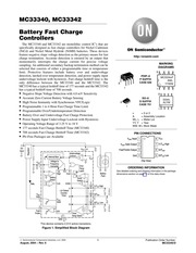
27. vailable 5 e i 3 8 m Input 5 24 2 Undervoltage T 1 Internal Bias Lockout TL 3 2 gE Voc Voltage to Frequency Converter Over Temp Ck FN Latch 2 2 Migh Over 0 e Battery Pack nad Temp eteci Detect 4 4 Low Under 5 t1 Tret High ti lt lo 2 AV Detect 7 Counter i lI Timer I i V dex dl 13 Trep Low Bh Po Tio HE VT Time GND 94 This device contains 2 512 active transistors Figure 1 Simplified Block Diagram Semiconductor Components Industries LLC 2004 1 August 2004 Rev 6 ON Semiconductor http onsemi com MARKING DIAGRAMS PDIP 8 j j P SUFFIX MC3334xP 8 CASE 626 1 SO 8 8 AS D SUFFIX CASE 751 X 00 2 Assembly Location WL L Wafer Lot YY Y Year WW W Work Week PIN CONNECTIONS Veen Input Voc Vsen Gate Output t1 Tre High Fast Trickle Output t2 Tsen Gnd Low Top View ORDERING INFORMATION See detailed ordering and shipping information in the package dimensions section on pagp of this data sheet Publication Order Number MC33340 D MC33340 MC33342 MAXIMUM RATINGS Note 1 Rating Symbol Value Unit Power Supply Voltage Pin 8
Download Pdf Manuals

Related Search
ON SEMICONDUCTOR MC33340 MC33342 handbook(1)