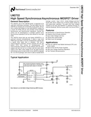
NATIONAL SEMICONDUCTOR -LM2722 High Speed Synchronous/Asynchronous MOSFET Driver handbook
Contents
1. 193 004 4 9 0 1 OTE 236 t 008 5 9920 2 050 TP 1 27 069 MAX 057 1 175 ias C TYP c 004 0 1 i E 0138 0200 TYP 004 010 0 35 0 51 0 10 0 25 TYP R 0072 001 0 18 0 02 R 0092 001 0 2330 02 016 050 SEATING PLANE J 0 41 1 27 042 1 07 DETAIL A TYPICAL SCALE 40X JCLR x N e e SEE DETAIL A 4L 0075 0098 0 19 0 25 TYP CONTROLLING DIMENSION IS INCH VALUES IN ARE MILLIMETERS MOBA Rev J 8 Lead Small Outline Package NS Package Number M08A LIFE SUPPORT POLICY NATIONAL S PRODUCTS ARE NOT AUTHORIZED FOR USE AS CRITICAL COMPONENTS IN LIFE SUPPORT DEVICES OR SYSTEMS WITHOUT THE EXPRESS WRITTEN APPROVAL OF THE PRESIDENT AND GENERAL COUNSEL OF NATIONAL SEMICONDUCTOR CORPORATION As used herein 1 Life support devices or systems are devices or systems which a are intended for surgical implant into the body or b support or sustain life and whose failure to perform when properly used in accordance with instructions for use provided in the labeling can be reasonably expected to result in a significant injury to the user N www national com National Semiconductor National Semiconductor Corporation Europe Americas Fax 49 0 180 530 85 86 Email support nsc com Email europe support nsc com Deutsch Tel 49 0 69 9508 6208 English Tel 44 0 870 24 0 2171 Fran ais Tel 33 0 1 41 91 8790 2 A critical com2. IN Accepts a 5V logic control signal SYNC EN Low gate Enable Connect to 5V supply Bottom gate drive output Ground Q co o o A2 o lt r I Oo O Z UO www national com 2 Block Diagram TAN 7V Q Vn up to 35V z l E SYNC EN LG Items in bold are external Shoot through to the IC Protection GND 20028904 www national com ccLoW 1l LM2722 Absolute Maximum Ratings Note 1 Storage Temperature 65 to 150 C If Military Aerospace specified devices are required ESD Susceptibility please contact the National Semiconductor Sales Office Human Body Model Note 3 1kV Distributors for availability and specifications Soldering Time Temperature 10sec 300 C VCC 7 5V GRUHI Aay Operating Ratings Note 1 CBOOT to SW 8V SW to PGND 36V Ye cO Junction Temperature 4150 C Junction Temperature Range 40 to 125 C Power Dissipation Note 2 720mW Electrical Characteristics VCC CBOOT 5V SW GND OV unless otherwise specified Typicals and limits appearing in plain type apply for T4 T 25 C Limits appearing in boldface type apply over the entire operating temperature range POWER SUPPLY MES Operating Quiescent PWM IN OV 190 uA Current TOP DRIVER Peak Pull Up Current Test Circuit 1 Vbias 5V R 0 10 Pull Up Rds_on lcBoor luc 0 7A Peak Pull down Current Test Circuit 2 Vbias 5V R 0 10 Pull down Rds on law lug 0 7A ts Pull Up Dead Time Timing Diagra
3. One Shot Test Circuit 2 CBOOT SYNC_EN vcc PWM IN GND Width 200ns One Shot Test Circuit 4 P as pull_up d V bias Hae pull down V 20028908 Typical Waveforms Chi 5 00V Ch2 5 00V M 400ns A Chi J 2 70V Ch3 5 00V 20028913 FIGURE 1 Switching Waveforms of Test Circuit EX LT es P rS Ch1 5 00V Ch2 2 00V M 20 0ns A Chi J 2 70V Ch3 2 00V 20028914 FIGURE 2 When Input Goes High Application Information Minimum Pulse Width In order for the shoot through prevention circuitry in the LM2722 to work properly the pulses into the PWM IN pin must be longer than 55ns The internal logic waits until the first FET is off plus 20ns before turning on the opposite FET If after a falling edge a rising edge occurs sooner than the specified time tor mins the IC may intermittently fail to turn on the top gate when the bottom gate is off As the rising edge occurs sooner and sooner the driver may start to ignore the pulse and produce no output This condition results in the PWM_IN pin in a high state and neither FET turned on To get out of this state the PWM_IN pin must see a low signal for greater than 55ns before the rising edge This will also assure that the gate drive bias voltage has been restored by forcing the top FET source and Choot to ground first Then the internal circuitry is reset and normal operation will resume Conversely if after a rising edge a falling edge occurs soon
4. M National Semiconductor LM2722 December 2001 High Speed Synchronous Asynchronous MOSFET Driver General Description The LM2722 part of the LM2726 family is designed to be used with multi phase controllers This part differs from the LM2726 by changing the functionality of the SYNC_EN pin from a whole chip enable to a low side MOSFET enable As a result the SYNC_EN pin now provides control between Synchronous and Asynchronous operations Having this control can be advantageous in portable systems since Asynchronous operations can be more efficient at very light loads The LM2722 drives both top and bottom MOSFETs in a push pull structure simultaneously It takes a logic level PWM input and splits it into two complimentary signals with a typical 20ns dead time in between The built in cross conduction protection circuitry prevents the top and bottom FETs from turning on simultaneously The cross conduction protection circuitry detects both the driver outputs and will not turn on a driver until the other driver output is low With a bias voltage of 5V the peak sourcing and sinking current for each driver of the LM2722 is typically 3A In an SO 8 package each driver is able to handle 50mA Typical Application average current Input UVLO Under Voltage Lock Out forces both driver outputs low to ensure proper power up and power down operation The gate drive bias voltage needed by the high side MOSFET is obtained through an externa
5. able power dissipation is a function of the maximum junction temperature T juAx the junction to ambient thermal resistance 0 4 and the ambient temperature Ta The maximum allowable power dissipation at any ambient temperature is calculated using Pmax Tymax Ta Oya The junction to ambient thermal resistance 0 4 for the LM2722 it is 172 C W For a Tjmax of 150 C and T4 of 25 C the maximum allowable power dissipation is 0 7W Note 3 ESD machine model susceptibility is 100V Note 4 If after a rising edge a falling edge occurs sooner than the specified value the IC may intermittently fail to turn on the bottom gate when the top gate is off As the falling edge occurs sooner and sooner the driver may start to ignore the pulse and produce no output Note 5 If after a falling edge a rising edge occurs sooner than the specified value the IC may intermittently fail to turn on the top gate when the bottom gate is off As the rising edge occurs sooner and sooner the driver may start to ignore the pulse and produce no output Timing Diagram SYNC EN 20028903 5 www national com ccLoW 1 LM2722 Test Circuits CBOOT Viis SYNC_EN VCC sw PWM IN GND Width 200ns One Shot 20028905 Test Circuit 1 CBOOT bias SYNC EN J Ue 3 PwMIN GND Width 200ns One Shot 20028907 Test Circuit 3 DM pul up R V bias x V pull down R www national com HG LG SW GND Width 200ns
6. er than the specified miniumum pulse width to min the g MT TT SE DEM Sm im Chi 5 00V Ch2 2 00V M 20 0ns A Chi J 2 70V Ch3 2 00V 20028915 FIGURE 3 When Input Goes Low Ch1 5 00V Ch2 2 00V M 20 0ns A Chi J 2 70V Ch3 2 00V 20028916 FIGURE 4 Minimum Positive Pulse IC may intermittently fail to turn on the bottom FET As the falling edge occurs sooner and sooner the driver will start to ignore the pulse and produce no output This will result in the tog inductor current taking a path through a diode provided for non synchronous operation The circuit will resume syn chronous operation when the rising PWM pulses exceed 55ns in duration High Input Voltages or High Output Currents At input voltages above twice the output voltage and at higher power levels the designer may find snubber networks and gate drive limiting useful in reducing EMI and preventing injurious transients A small resistor 1O to 5O between the driver outputs and the MOSFET gates will slightly increase the rise time and fall time of the output stage and reduce switching noise The trade off is 1 to 2 in efficiency A series R C snubber across in parallel with the bottom FET can also be used to reduce ringing Values of 10nF and 10Q to 1000 are a good starting point www national com ccLoW 1 LM2722 High Speed Synchronous Asynchronous MOSFET Driver Physical Dimensions inches millimeters unless otherwise noted
7. l bootstrap Minimum pulse width is as low as 55ns Features m Synchronous or Asynchronous Operation m Adaptive shoot through protection m Input Under Voltage Lock Out m Typical 20ns internal delay m Plastic 8 pin SO package Applications m Driver for LM2723 Intel Mobile Northwood CPU core power supply m High Current DC DC Power Supplies m High Input Voltage Switching Regulators m Fast Transient Microprocessors Note for ultra low frequency operation such as skip mode at light load D should be a fast recovery type diode instead of a Schottky C 2 1uF l vcc cBoor L3 SYNC EN SIGNALS PWMSIGNAL 4 LM2722 Note National is an Intel Mobile Voltage Positioning IMVP licensee 2001 National Semiconductor Corporation DS200289 45 10 D Aa Vp up to 35V T Cw C oF EE a L Vour T Cour 20028901 www national com JOAUGQ LAASOIN Snououugou sy snououqou AS peeds yH ZZZZIN7 LM2722 Connection Diagram 8 Lead Small Outline Package SW GND HG LG CBOOT vec PWM IN SYNC EN 20028902 Top View Ordering Information Order Number Package Type NSC Package Drawing Supplied As LM2722M 95 Units Rail LM2722 M08A LM2722MX 2500 Units Reel Pin Description Pin Function Top driver return Should be connected to the common node of top i and bottom FETs 2 G Top gate drive output CBOOT Bootstrap Accepts a bootstrap voltage for powering the high side driver PWM
8. m t5 Pull Down Delay Timing Diagram from PWM IN Falling Edge BOTTOM DRIVER Peak Pull Up Current Test Circuit 3 V4 5V R 0 10 Pull up Rds on lvcc lic 0 7A Peak Pull down Current Test Circuit 4 Vbias 5V R 0 10 Pull down Rds_on lanp lia 0 7A 3 Timing Diagram Croan te Fall Time 3 3nF t Pull up Dead Time Timing Diagram t Pull down Delay Timing Diagram from PWM IN Rising Edge V ouod Power On Threshold VCC rises from OV toward 5V V uie an Under Voltage Lock Out Threshold Vinischye Under Voltage Lock Out Hysteresis Via eR SYNC EN Pin High Input TER SYNC EN Pin Low Input www national com 4 Electrical Characteristics continued VCC CBOOT 5V SW GND OV unless otherwise specified Typicals and limits appearing in plain type apply for T4 Ty 25 C Limits appearing in boldface type pews over the entire operating temperature ee Symbol leak EN SYNC_EN Pin Leakage Current tonm Minimum Positive Input Pulse Width Note 4 toffi _min Minimum Negative Input Pulse Width Note 5 Vin Pwo PWM IN High Level Input When PWM IN pin goes Voltage high from OV Vii PwM PWM IN Low Level Input When PWM IN pin goes Voltage low from 5V Note 1 Absolute Maximum Ratings are limits beyond which damage to the device may occur Operating ratings are conditions under which the device operates correctly Operating Ratings do not imply guaranteed performance limits Note 2 Maximum allow
9. ponent is any component of a life support device or system whose failure to perform can be reasonably expected to cause the failure of the life support device or system or to affect its safety or effectiveness National Semiconductor Japan Ltd Tel 81 3 5639 7560 Fax 81 3 5639 7507 National Semiconductor Asia Pacific Customer Response Group Tel 65 2544466 Fax 65 2504466 Email ap support nsc com National does not assume any responsibility for use of any circuitry described no circuit patent licenses are implied and National reserves the right at any time without notice to change said circuitry and specifications
Download Pdf Manuals

Related Search