ANALOG DEVICES AD823 Manual(3)
Contents
1. 0 6 5 4 3 2 1 0 1 2 3 4 5 6 7 INPUT OFFSET VOLTAGE DRIFT uV C 00901 009 TEMPERATURE C 00901 006 Figure 6 Typical Distribution of Input Offset Voltage Drift Figure 9 Input Bias Current vs Temperature 1000 INPUT BIAS CURRENT pA S INPUT BIAS CURRENT pA 4 5 4 3 2 1 0 1 2 3 4 5 COMMON MODE VOLTAGE V 00901 007 00901 010 COMMON MODE VOLTAGE V Figure 7 Input Bias Current vs Common Mode Voltage Figure 10 Input Bias Current vs Common Mode Voltage Rev B Page 7 of 20 AD823 OPEN LOOP GAIN dB THD dB 110 100 90 80 k 10k 100k 500k LOAD RESISTANCE Q Figure 11 Open Loop Gain vs Load Resistance e e e Ri 10kO ETE EET o a SaaS 2 5 2 0 1 5 1 0 05 0 05 10 15 2 0 OUTPUT VOLTAGE V Figure 12 Open Loop Gain vs Output Voltage Vs 2 5 V 40 4 50 P M o 90 v aav 7 Vout 2V p p 5 70 R 1000 A nS 80 Vg 2 5V Vs 15V Vour aV BP A s mE 90 L Vour 10V p p t Vour 2V p p R 6000 j REZSO 100 cedi d Vg 5V m n Vout 2V p p RL 5kQ 110 100 1k 10k 100k 1M FREQUENCY Hz Figure 13 Total Harmonic Distortion vs Frequency2. 00901 004 AMBIENT TEMPERATURE C Figure 4 Maximum Power Dissipation vs Temperature THERMAL RESISTANCE Oya is specified for the worst case conditions that is a device soldered in a circuit board for surface mount packages Specification is for device in free air Table 5 Thermal Resistance Package Type Osa Unit 8 Lead PDIP 90 C W 8 Lead SOIC 160 C W ESD CAUTION A ISEN ESD electrostatic discharge sensitive device Charged devices and circuit boards can discharge without detection Although this product features patented or proprietary protection circuitry damage may occur on devices subjected to high energy ESD Therefore proper ESD precautions should be taken to avoid performance degradation or loss of functionality Rev B Page 6 of 20 AD823 TYPICAL PERFORMANCE CHARACTERISTICS 100 Vs 5V TVs 5V 314 UNITS 90 317 UNITS o 40V UNITS UNITS a o 0 1 2 3 4 5 6 7 8 9 10 INPUT BIAS CURRENT pA 0 200 150 100 50 0 50 100 150 200 INPUT OFFSET VOLTAGE uV 00901 005 00901 008 Figure 5 Typical Distribution of Input Offset Voltage Figure 8 Typical Distribution of Input Bias Current Vg 5V 55 C TO 125 C 103 UNITS UNITS
3. sees 15 Outline Dimensions eite tento iet tinet tebi test es itta 18 Ordering Guide oe ep RO deett es 19 Rev B Page 2 of 20 SPECIFICATIONS At Ta 25 C Vs 5 V Rr 2 kQ to 2 5 V unless otherwise noted AD823 Table 1 Parameter Conditions Min Typ Max Unit DYNAMIC PERFORMANCE 3 dB Bandwidth Vo lt 0 2 V p p G 241 12 16 MHz Full Power Response Vo 2 V p p 3 5 MHz Slew Rate G 1 Vo 4V Step 14 22 V us Settling Time to 0 196 G 1 Vo 2V Step 320 ns to 0 0196 G 1 Vo 2V Step 350 ns NOISE DISTORTION PERFORMANCE Input Voltage Noise f 10kHz 16 nV 4Hz Input Current Noise f 1kHz 1 fA VHz Harmonic Distortion R 600 O to 2 5 V Vo 2 V p p f 20 kHz 108 dBc Crosstalk f 1 kHz R 25kQ 105 dB f 1 MHz RL 5kO 63 dB DC PERFORMANCE Initial Offset 0 2 0 8 mV Maximum Offset Over temperature 0 3 2 0 mV Offset Drift 2 yv C Input Bias Current Vcu 2 OVto AV 3 25 pA at Tmax Vcn 2 OVto AV 0 5 5 nA Input Offset Current 2 20 pA at Tmax 0 5 nA Open Loop Gain Vo 0 2V to 4V RL 2kO 20 45 V mV Tmn to Tmax 20 V mV INPUT CHARACTERISTICS Input Common Mode Voltage Range 0 2 to 3 0 2to 43 8 V Input Resistance 10 Q Input Capacitance 1 8 pF Common Mode Rejection Ratio Vcn 2 OV to 3V 60 76 dB OUTPUT CHARACTERISTICS Output Voltage Swing IL 100 uA 0 025 to 4 975 V IL 2mA 0 08 to 4 92 V IL 10 mA 0 25 to 4 75 V Output Current Vour 0 5 V to 4 5 V 16 mA Short Circuit Current Sou
4. 00901 011 00901 012 00901 013 Rev B Page 8 of 20 OPEN LOOP GAIN dB 55 25 5 35 65 95 125 TEMPERATURE C Figure 14 Open Loop Gain vs Temperature 100 60 40 20 OPEN LOOP GAIN dB PHASE MARGIN Degrees 20 100 1k 10k 100k 1M 10M 100M FREQUENCY Hz Figure 15 Open Loop Gain and Phase Margin vs Frequency INPUT VOLTAGE NOISE nV VHz 3 10 100 1k 10k 100k FREQUENCY Hz Figure 16 Input Voltage Noise vs Frequency 00901 014 00901 016 00901 015 T 2 z a o n rm se o z N 4 ENS W o l N o 70 30 3 27 6 24 9 21 12 18 15 15 18 12 21 09 24 06 27 03 30 00 FREQUENCY MHz Figure 17 Closed Loop Gain vs Frequency 100 Vg 45V GAIN 4 amp 10 ul o E o B 4 2 m 2 n E 2 O 01 0 01 100 1k 10k 100k 1M 10M FREQUENCY Hz 00901 017 00901 018 Figure 18 Output Resistance vs Frequency Vs 5 V Gain 1 OUTPUT STEP SIZE FROM 0V TO Vsuoww V e 100 200 300 400 500 600 700 SETTLING TIME ns Figure 19 Output Step Size vs Settling Time Inverter 00901 019 Rev B Page 9 of 20 CMRR dB OUTPUT SATURATION VOLTAGE V QUIESCE
5. IL 10 mA 0 25 to 3 05 V Output Current Vout 0 5 V to 2 5 V 15 mA Short Circuit Current Sourcing to 1 5 V 40 mA Sinking to 1 5 V 30 mA Capacitive Load Drive G 1 500 pF POWER SUPPLY Operating Range 3 36 V Quiescent Current Tmn to Tmax total 5 0 5 7 mA Power Supply Rejection Ratio Vs 3 3 V to 15 V Tmn to Tmax 70 80 dB Rev B Page 4 of 20 At Ta 25 C Vs 15 V Ru 2 KO to 0 V unless otherwise noted AD823 Table 3 Parameter Conditions Min Typ Max Unit DYNAMIC PERFORMANCE 3 dB Bandwidth Vo lt 0 2 V p p G 41 12 16 MHz Full Power Response Vo 2 V p p 4 MHz Slew Rate G 1 Vo 10V Step 17 25 V us Settling Time to 0 196 G 1 Vo 10V Step 550 ns to 0 01 G 1 Vo 10V Step 650 ns NOISE DISTORTION PERFORMANCE Input Voltage Noise f 10 kHz 16 nV VHz Input Current Noise f 1kHz 1 fA VHz Harmonic Distortion Ri 600 Q Vo 10 V p p f 20 kHz 90 dBc Crosstalk f 1 kHz R 5 kQ 105 dB f 1 MHz R 5 kQ 63 dB DC PERFORMANCE Initial Offset 0 7 3 5 mV Maximum Offset Over temperature 1 0 7 mV Offset Drift 2 uV C Input Bias Current Vem 0V 5 30 pA Vem 2 10 V 60 pA at Tmax Vem 0V 0 5 5 nA Input Offset Current 2 20 pA at Tmax 0 5 nA Open Loop Gain Vo 10V to 10V R 2 kQ 30 60 V mV Tmn to Tmax 30 V mV INPUT CHARACTERISTICS Input Common Mode Voltage Range 15 2to 413 15 2to 13 8 V Input Resistance 1055 Q Input Capacitance 1 8 pF Common Mode Reje
6. exhibits good current drive and total harmonic distortion plus noise THD N performance even at 3 V single supplies At 20 kHz THD N equals 62 dB 0 079 for a 300 mV p p output signal This is comparable to other single supply op amps that consume more power and cannot run on 3 V power supplies In Figure 42 each channel s input signal is coupled via a 1 uF Mylar capacitor Resistor dividers set the dc voltage at the noninverting inputs so that the output voltage is midway between the power supplies 41 5 V The gain is 1 5 Each half ofthe AD823 can then be used to drive a headphone channel A 5 Hz high pass filter is realized by the 500 uF capacitors and the headphones that can be modeled as 32 Q load resistors to ground This ensures that all signals in the audio frequency range 20 Hz to 20 kHz are delivered to the headphones 3v 95 3kQ CHANNEL 1 0 1uF MYLAR 95 3kO HEADPHONES 320 IMPEDANCE 1pF CHANNEL 2 O MYLAR 00901 042 Figure 42 3 V Single Supply Stereo Headphone Driver Rev B Page 16 of 20 Second Order Low Pass Filter Figure 43 depicts the AD823 configured as a second order Butterworth low pass filter With the values as shown the corner frequency equals 200 kHz Component selection is shown in the following equations R1 R2 User Selected Typical Values 10 KO to 100 kQ Cl farads C2 A plot of the filter is shown in Figure 44 better than 50 dB of 1 414 2n
7. 40 C to 85 C and is offered in both 8 lead PDIP and 8 lead SOIC packages One Technology Way P O Box 9106 Norwood MA 02062 9106 U S A Tel 781 329 4700 www analog com Fax 781 461 3113 1995 2007 Analog Devices Inc All rights reserved AD823 TABLE OF CONTENTS Features oce eoe LU Le uer 1 Applications iiie venen bei en e ori eR USE 1 General Descriptions zsctseiessscsssevesessvatevebscetvcehidenstsbevessdebsienodesotevenesy 1 Connection Diagram sse 1 REVISION HIStory eee RR ERBEN RR ted es 2 Sp cifications see a R E EE t ae 3 Absolute Maximum Ratings essent 6 Thermal Resistaticez s eot erit te pite nete e etait 6 BSDCAUtlOTL 2r tereti te o EK 6 REVISION HISTORY 2 07 Rev A to Rev B Updated Format Universal Changes to DC Performance sse 5 Updated Outline Dimensions eerte 18 Changes to Ordering Guide sse 19 5 04 Rev 0 to Rev A Changes to Specifications 2 Changes to Ordering Guide sse 17 Updated Outline Dimensions seen 17 5 95 Revision 0 Initial Version Typical Performance Characteristics sse 7 Theory of Operation nee eene Pierii creen 13 Output Impedanc u s iecit entretenu venere eene 14 Application Notes m er nt eR dieere 15 Input Characteristics cesesessesessessessesssesessessesessessesseesees 15 Output Characteristics
8. 500 0 10 SEATING 317100067 0 40 0 0157 PLANE 0 17 0 0067 40 0 COMPLIANT TO JEDEC STANDARDS MS 012AA CONTROLLING DIMENSIONS ARE IN MILLIMETERS INCH DIMENSIONS IN PARENTHESES ARE ROUNDED OFF MILLIMETER EQUIVALENTS FOR REFERENCE ONLY AND ARE NOT APPROPRIATE FOR USE IN DESIGN Figure 48 8 Lead Standard Small Outline Package SOIC_N Narrow Body R 8 Dimensions shown in millimeters and inches Rev B Page 18 of 20 AD823 ORDERING GUIDE Models Temperature Range Package Description Package Option AD823AN 40 C to 85 C 8 Lead PDIP N 8 AD823ANZ 40 C to 85 C 8 Lead PDIP N 8 AD823AR 40 C to 85 C 8 Lead SOIC_N R 8 AD823AR REEL 40 C to 85 C 8 Lead SOIC_N 13 Reel R 8 AD823AR REEL7 40 C to 85 C 8 Lead SOIC_N 7 Reel R 8 AD823ARZ 40 C to 85 C 8 Lead SOIC_N R 8 AD823ARZ RL 40 C to 85 C 8 Lead SOIC N 13 Reel R 8 AD823ARZ R7 40 C to 85 C 8 Lead SOIC_N 7 Reel R 8 1 Z RoHS Compliant Part Rev B Page 19 of 20 AD823 NOTES 1995 2007 Analog Devices Inc All rights reserved Trademarks and ANALOG registered trademarks are the property of their respective owners C00901 0 2 07 B DEVICES www analo g com Rev B Page 20 of 20
9. 9 00901 030 00901 031 Rev B Page 11 of 20 TEDT TETT Te rT BEESEREENE STORET NENEEERPNE Figure 34 Pulse Response Vs 5V G 1 C 470 pF 00901 034 00901 032 00901 033 A CRINE Figure 35 Pulse Response Vs 15 V G 1 00901 035 Rev B Page 12 of 20 THEORY OF OPERATION The AD823 is fabricated on the Analog Devices Inc proprietary complementary bipolar CB process that enables the construction of PNP and NPN transistors with similar fr s in the 600 MHz to 800 MHz region In addition the process also features N Channel JFETs that are used in the input stage of the AD823 These process features allow the construction of high frequency low distortion op amps with picoamp input currents This design uses a differential output input stage to maximize bandwidth and headroom see Figure 36 The smaller signal swings required on the S1P S1N outputs reduce the effect of the nonlinear currents due to junction capacitances and improve the distortion performance With this design harmonic distortion of better than 91 dB 20 kHz into 600 Q with Vovr 4 V p p ona single 5 V supply is achieved The complementary common emitter design of the output stage provides excellent load drive without the need for emitter followers thereby improving the output range of the device considerably with respect to conventional op amps The AD823 can drive 20 mA with the outputs within 0 6 V of the supply rail
10. ANALOG DEVICES Dual 16 MHz Rail to Rail FET Input Amplifier AD823 FEATURES Single supply operation Output swings rail to rail Input voltage range extends below ground Single supply capability from 3 V to 36 V High load drive Capacitive load drive of 500 pF G 1 Output current of 15 mA 0 5 V from supplies Excellent ac performance on 2 6 mA amplifier 3 dB bandwidth of 16 MHz G 1 350 ns settling time to 0 0196 2 V step Slew rate of 22 V us Good dc performance 800 uV maximum input offset voltage 2 pV C offset voltage drift 25 pA maximum input bias current Low distortion 108 dBc worst harmonic 20 kHz Low noise 16 nV VHz 10 kHz No phase inversion with inputs to the supply rails APPLICATIONS Battery powered precision instrumentation Photodiode preamps Active filters 12 bit to 16 bit data acquisition systems Medical instrumentation GENERAL DESCRIPTION The AD823 is a dual precision 16 MHz JFET input op amp that can operate from a single supply of 3 0 V to 36 V or from dual supplies of 1 5 V to 18 V It has true single supply capability with an input voltage range extending below ground in single supply mode Output voltage swing extends to within 50 mV of each rail for Iovr 100 uA providing outstanding output dynamic range An offset voltage of 800 uV maximum an offset voltage drift of 2 uV C input bias currents below 25 pA and low input voltage noise provide dc precision with source imped
11. NT CURRENT mA AD823 HEAS 40 L gt 30 20 10 100 1k 10k 100k 1M 10M FREQUENCY Hz Figure 20 Common Mode Rejection Ratio vs Frequency 0 1 1 10 100 LOAD CURRENT mA Figure 21 Output Saturation Voltage vs Load Current 125C 0 5 10 15 20 SUPPLY VOLTAGE V Figure 22 Quiescent Current vs Supply Voltage 00901 020 00901 021 00901 022 POWER SUPPLY REJECTION dB OUTPUT VOLTAGE V p p 0 100 1k 10k 100k FREQUENCY Hz Figure 23 Power Supply Rejection vs Frequency FREQUENCY Hz Figure 24 Large Signal Frequency Response Figure 25 Output Swing Vs 3 V V G 1 00901 025 00901 023 00901 024 Rev B Page 10 of 20 N oo a N o o SERIES RESISTANCE Q CAPACITOR pF x 1000 Figure 26 Series Resistance vs Capacitive Load Vg 65V CROSSTALK dB 5 e 1k 10k 100k 1M 10M FREQUENCY Hz Figure 27 Crosstalk vs Frequency 00901 028 Figure 28 Output Swing Vs X15 V G 1 00901 026 00901 027 FAL PT tT UAT a tT i EAA ES NA EE eA RECS RE Figure 29 Output Swing Vs 5 V G 1 Figure 31 Pulse Response Vs 5 V G 42 00901 02
12. T IMPEDANCE The low frequency open loop output impedance of the common emitter output stage used in this design is approximately 30 kQ Although this is significantly higher than a typical emitter follower output stage when it is connected with feedback the output impedance is reduced by the open loop gain of the op amp With 109 dB of open loop gain the output impedance is reduced to 0 2 At higher frequencies the output impedance rises as the open loop gain of the op amp drops however the Figure 37 Small Signal Schematic output also becomes capacitive due to the integrator capacitors C1 and C2 This prevents the output impedance from ever becoming excessively high see Figure 18 which can cause stability problems when driving capacitive loads In fact the AD823 has excellent cap load drive capability for a high frequency op amp Figure 34 shows the AD823 connected as a follower while driving 470 pF direct capacitive load Under these conditions the phase margin is approximately 20 If greater phase margin 00901 037 is desired a small resistor can be used in series with the output to decouple the effect of the load capacitance from the op amp see Figure 26 In addition running the part at higher gains also improves the capacitive load drive capability of the op amp Rev B Page 14 of 20 APPLICATION NOTES INPUT CHARACTERISTICS In the AD823 N Channel JFETs are used to provide a low offset low noise h
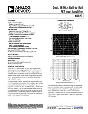
13. ances up to a Gigaohm It provides 16 MHz 3 dB bandwidth 108 dB THD 20 kHz and a 22 V us slew rate with a low supply current of 2 6 mA per amplifier The AD823 drives up to 500 pF of direct capacitive load as a follower and provides an output current of 15 mA 0 5 V from the supply rails This allows the amplifier to handle a wide range of load conditions Rev B Information fumished by Analog Devices is believed to be accurate and reliable However no responsibility is assumed by Analog Devices for its use nor for any infringements of patents or other rights ofthird parties that may result fromits use Specifications subjectto change without notice No license is granted by implication or otherwise under any patent or patent rights of Analog Devices Trademarks and registered trademarks are the property of their respective owners CONNECTION DIAGRAM 00901 001 00901 002 Figure 2 Output Swing Vs 3 V G 1 Vs 5V 1 G 1 OUTPUT dB b 8 1k 10k 100k 1M 10M FREQUENCY Hz Figure 3 Small Signal Bandwidth G 1 00901 003 This combination of ac and dc performance plus the outstanding load drive capability results in an exceptionally versatile ampli fier for applications such as A D drivers high speed active filters and other low voltage high dynamic range systems The AD823 is available over the industrial temperature range of
14. as heavily low pass filtered 60 dB to minimize the harmonic content at the input to the AD823 The digital output of the AD1672 was analyzed by performing a fast Fourier transform FFT During the testing it was observed that at 500 kHz the output of the AD823 cannot go below 350 mV operating with negative supply at ground without seriously degrading the second harmonic distortion Another test was performed with a 200 Q pull down resistor to ground that allowed the output to go as low as 200 mV without seriously affecting the second harmonic distortion There was however a slight increase in the third harmonic term with the resistor added but it was still less than the second harmonic Figure 41 is an FFT plot of the results of driving the AD1672 with the AD823 with no pull down resistor The input amplitude was 2 15 V p p and the lower voltage excursion was 350 mV The input frequency was 490 kHz which was chosen to spread the location of the harmonics The distortion analysis is important for systems requiring good frequency domain performance Other systems may require good time domain performance The noise and settling time performance of the AD823 provides the necessary information for its applicability for these systems Vin 2 15V p p G 1 FI 490kHz 15dB DIV 00901 041 Figure 41 FFT of AD1672 Output Driven by AD823 3 V Single Supply Stereo Headphone Driver The AD823
15. ction Ratio Vem 15Vto 13V 66 82 dB OUTPUT CHARACTERISTICS Output Voltage Swing IL 100 pA 14 95 to 14 95 V IL 2mA 14 92 to 14 92 V IL 10mA 14 75 to 14 75 V Output Current Vout 14 5 V to 14 5 V 17 mA Short Circuit Current Sourcing to 0 V 80 mA Sinking to 0 V 60 mA Capacitive Load Drive G 1 500 pF POWER SUPPLY Operating Range 3 36 V Quiescent Current Tmn to Tmax total 7 0 8 4 mA Power Supply Rejection Ratio Vs 5V to 15 V Tmn to Tmax 70 80 dB Rev B Page 5 of 20 AD823 ABSOLUTE MAXIMUM RATINGS Table 4 Parameter Rating Supply Voltage 36V Internal Power Dissipation PDIP N 1 3 W SOIC R 0 9W Input Voltage Common Mode TVs Differential Input Voltage 1 2V Output Short Circuit Duration See Figure 4 Storage Temperature Range N R 65 C to 125 C Operating Temperature Range 40 C to 85 C Lead Temperature Range 300 C Soldering 10 sec Stresses above those listed under Absolute Maximum Ratings may cause permanent damage to the device This is a stress rating only functional operation of the device at these or any other conditions above those indicated in the operational section of this specification is not implied Exposure to absolute maximum rating conditions for extended periods may affect device reliability 2 0 a Ty 150 C LEAD PDIP a MAXIMUM POWER DISSIPATION W o 0 50 40 30 20 10 0 10 20 30 40 50 60 70 80 90
16. f cutoff x RI 0 707 i 2nf ug X RI Figure 43 Second Order Low Pass Filter high frequency rejection is provided HIGH FREQUENCY REJECTION dB 0 1 o Vos Vout 40 10k 100k 1M 10M FREQUENCY Hz Figure 44 Frequency Response of Filter 100M 00901 043 00901 044 AD823 Single Supply Half Wave and Full Wave Rectifiers An AD823 configured as a unity gain follower and operated with a single supply can be used as a simple half wave rectifier The AD823 inputs maintain picoamp level input currents even when driven well below the minus supply The rectifier puts that behavior to good use maintaining an input impedance of over 10 Q for input voltages from within 1 V of the positive supply to 20 V below the negative supply The full wave and half wave rectifier shown in Figure 45 operates as follows when Vix is above ground R1 is boot strapped through the unity gain follower A1 and the loop of Amplifier A2 This forces the inputs of A2 to be equal thus no current flows through R1 or R2 and the circuit output tracks the input When Vn is below ground the output of A1 is forced to ground The noninverting input of Amplifier A2 sees the ground level output of A1 therefore A2 operates as a unity gain inverter The output at Node C is then a full wave rectified version of the input Node B is a buffered half wave rectified version
17. igh impedance input stage Minimum input common mode voltage extends from 0 2 V below Vs to 1 V lt Vs Driving the input voltage closer to the positive rail causes a loss of amplifier bandwidth and increased common mode voltage error The AD823 does not exhibit phase reversal for input voltages up to and including Vs Figure 38 shows the response of an AD823 voltage follower to a 0 V to 5 V Vs square wave input The input and output are superimposed The output polarity tracks the input polarity up to Vs with no phase reversal The reduced bandwidth above a 4 V input causes the rounding of the output wave form For input voltages greater than Vs a resistor in series with the AD823 s noninverting input prevents phase reversal at the expense of greater input voltage noise This is illustrated in Figure 39 00901 038 00901 039 Figure 39 AD823 Input Response Viu 0 to Vs 200 mV Vout 0 to Vs Re 49 9 kQ AD823 Because the input stage uses N Channel JFETs input current during normal operation is negative the current flows out from the input terminals If the input voltage is driven more positive than Vs 0 4 V the input current reverses direction as internal device junctions become forward biased This is illustrated in Figure 7 A current limiting resistor should be used in series with the input of the AD823 if there is a possibility of the input voltage exceeding the positive supply by more than 300
18. inst the output saturation voltage it recovers within 250 ns of the input returning to the amplifier linear operating region A D Driver The rail to rail output of the AD823 makes it useful as an A D driver in a single supply system Because it is a dual op amp it can be used to drive both the analog input of the A D as well as its reference input The high impedance FET input of the AD823 is well suited for minimal loading of high output impedance devices Rev B Page 15 of 20 AD823 Figure 40 shows a schematic of an AD823 being used to drive both the input and reference input of an AD1672 a 12 bit 3 MSPS single supply ADC One amplifier is configured as a unity gain follower to drive the analog input of the AD1672 which is configured to accept an input voltage that ranges from 0 V to 2 5 V The other amplifier is configured as a gain of 2 to drive the reference input from a 1 25 V reference Although the AD1672 has its own internal reference there are systems that require greater accuracy than the internal reference provides On the other hand if the AD1672 internal reference is used the second AD823 amplifier can be used to buffer the reference voltage for driving other circuitry while minimally loading the reference source 5VA 5VD Vin O BIT12 LSB 00901 040 V Figure 40 AD823 Driving Input and Reference of the AD1672 a 12 Bit 3 MSPS ADC The circuit was tested with a 500 kHz sine wave input that w
19. mV or if an input voltage is applied to the AD823 when Vs 0 The amplifier becomes damaged if left in that condition for more than 10 seconds A 1 kQ resistor allows the amplifier to withstand up to 10 V of continuous overvoltage and increases the input voltage noise by a negligible amount Input voltages less than Vs are a completely different story The amplifier can safely withstand input voltages 20 V below Vs as long as the total voltage from the positive supply to the input terminal is less than 36 V In addition the input stage typically maintains picoamp level input currents across that input voltage range The AD823 is designed for 16 nV VHz wideband input voltage noise and maintains low noise performance to low frequencies see Figure 16 This noise performance along with the AD823 s low input current and current noise means that the AD823 contributes negligible noise for applications with source resistances greater than 10 kO and signal bandwidths greater than 1 kHz OUTPUT CHARACTERISTICS The AD8235 unique bipolar rail to rail output stage swings within 25 mV of the supplies with no external resistive load The AD823 s approximate output saturation resistance is 25 Q sourcing and sinking This can be used to estimate the output saturation voltage when driving heavier current loads For instance when driving 5 mA the saturation voltage to the rails is approximately 125 mV If the AD823 s output is driven hard aga
20. of the input Input voltage supply to 18 V can be rectified depending on the voltage supply used Cc Ot 1 2 FULL WAVE AD823 RECTIFIED OUTPUT B Jt Ga HALF WAVE RECTIFIED OUTPUT T Figure 45 Full Wave and Half Wave Rectifier 00901 044 00901 046 Figure 46 Single Supply Half Wave and Full Wave Rectifier Rev B Page 17 of 20 AD823 OUTLINE DIMENSIONS 0 375 9 53 0 365 9 27 0 355 9 02 t See eet 0 295 7 49 0 285 7 24 0 275 6 98 ae 0 325 8 26 X je 0 310 7 87 00 des 0 300 7 62 0 150 3 81 0 135 3 43 0 015 0 120 3 05 57 0 38 MAX MIN 0 015 0 38 0 150 3 81 s m 0 010 0 25 0 130 3 30 PLANE 0 008 0 20 0 110 2 79 0 060 1 52 0 022 0 56 0 050 1 27 0 018 0 46 0 045 1 14 0 014 0 36 COMPLIANT TO JEDEC STANDARDS MO 095AA CONTROLLING DIMENSIONS ARE IN INCHES MILLIMETER DIMENSIONS IN PARENTHESES ARE ROUNDED OFF INCH EQUIVALENTS FOR REFERENCE ONLY AND ARE NOT APPROPRIATE FOR USE IN DESIGN Figure 47 8 Lead Plastic Dual In Line Package PDIP Narrow Body N 8 Dimensions shown in inches and millimeters 5 00 0 1968 MS M 3 8 5 4 00 0 1574 6 20 0 2440 3 80 0 1497 T1 4 5 80 0 2284 quo gt fM 1 27 0 0500 0 50 0 0196 Bsc _ 1 75 0 0688 025 0 0099 0 25 0 0098 1 35 0 0532 0 10 0 0040 Y 1j LH a 0 51 0 0201 PE ke COPLANARITY 1 0 31 0 0122 0 25 0 0098 0 1 27 0 0
21. rcing to 2 5 V 40 mA Sinking to 2 5 V 30 mA Capacitive Load Drive G 1 500 pF POWER SUPPLY Operating Range 3 36 V Quiescent Current Tmn to Tmax total 5 2 5 6 mA Power Supply Rejection Ratio Vs 5V to 15 V Tmn to Tmax 70 80 dB Rev B Page 3 of 20 AD823 At Ta 25 C Vs 433 3 V Ri 2 kQ to 1 65 V unless otherwise noted Table 2 Parameter Conditions Min Typ Max Unit DYNAMIC PERFORMANCE 3 dB Bandwidth Vo x 0 2 V p p G 1 12 15 MHz Full Power Response Vo 2 V p p 3 2 MHz Slew Rate G 1 Vo 2 V Step 13 20 V us Settling Time to 0 196 G 1 Vo 2V Step 250 ns to 0 01 G 1 Vo 2V Step 300 ns NOISE DISTORTION PERFORMANCE Input Voltage Noise f 10 kHz 16 nV VHz Input Current Noise f 1kHz 1 fA VHz Harmonic Distortion Ri 100 O Vo 2 V p p f 20 kHz 93 dBc Crosstalk f 1 kHz R 25kQ 105 dB f 1 MHz RL 5kO 63 dB DC PERFORMANCE Initial Offset 0 2 1 5 mV Maximum Offset Over temperature 0 5 2 5 mV Offset Drift 2 uV C Input Bias Current Vcu 2 OV to 2V 3 25 pA at Tmax Vam O0Vto2V 0 5 5 nA Input Offset Current 2 20 pA at Tmax 0 5 nA Open Loop Gain Vo 0 2V to 2V RL 2kO 15 30 V mV Tmn to Tmax 12 V mV INPUT CHARACTERISTICS Input Common Mode Voltage Range 0 2 to 1 0 2 to 1 8 V Input Resistance 105 Q Input Capacitance 1 8 pF Common Mode Rejection Ratio Ven 2 OVto 1 V 54 70 dB OUTPUT CHARACTERISTICS Output Voltage Swing IL 100 uA 0 025 to 3 275 V IL 2mA 0 08 to 3 22 V
22. s The AD823 also offers outstanding precision for a high speed op amp Input offset voltages of 1 mV maximum and offset drift of 2 uV C are achieved through the use of the Analog Devices advanced thin film trimming techniques s _ Q53 i i Ra Vee O V 0 3V V1 v LL umm AD823 A nested integrator topology is used in the AD823 see Figure 37 The output stage can be modeled as an ideal op amp with a single pole response and a unity gain frequency set by transconductance gm and Capacitor C2 R1 is the output impedance of the input stage gm is the input transconductance C1 and C5 provide Miller compensation for the overall op amp The unity gain frequency occurs at gm C5 Solving the node equations for this circuit yields V our AO Vi smi CI A2 1 1 x J Ze S 4 where A0 gmgm2 R2R1 open loop gain of op amp A2 gw R2 open loop gain of output stage The first pole in the denominator is the dominant pole of the amplifier and occurs at 18 Hz This equals the input stage output impedance R1 multiplied by the Miller multiplied value of C1 The second pole occurs at the unity gain bandwidth of the output stage which is 23 MHz This type of architecture allows more open loop gain and output drive to be obtained than a standard 2 stage architecture would allow O Vour Q17 A 2 19 00901 036 Figure 36 Simplified Schematic Rev B Page 13 of 20 AD823 OUTPU
Download Pdf Manuals

Related Search
ANALOG DEVICES AD823 Manual(3) ic op amp ad823 ad7203 digital to analog converter ad820 single voltage op amp design ad8233 ecg circuit diagram ecg module ad8232 datasheet ad8232 library for arduino ad8302arz connect to 8302 ad8232 ecg sensor datasheet ad8232 ecg sensor circuit diagram analog discovery 2 ad2 analog.com ad8043 analog devices inc. adi ad8232 ecg sensor module adi analog devices inc modulo emg ad8832 datasheet