ST ST40RA handbook
Contents
1. Interrupt source INTEVT 1 77 IPR within ra p code bit numbers Value Initial value setting unit NMI Ox1CO 16 IRL IRLS IRLO F 0x200 15 E level IRL3 IRLO E 0x220 14 6 encoding IRLS IRLO D 0x240 13 IRLS IRLO C 0x260 12 2 IRL3 IRLO B 0x280 11 IRLS IRLO A 0x2A0 10 IRLS IRLO 9 0x2C0 9 IRLS IRLO 8 Ox2EO 8 IRLS IRLO 7 0x300 7 IRLS IRLO 6 0x320 6 IRLS IRLO 5 0x340 5 IRLS IRLO 4 0x360 4 IRLS IRLO 3 0x380 3 IRLS IRLO 2 0x3A0 2 IRLS IRLO 1 Ox3CO 1 IRL IRLO 0x240 15to0 13 IPRD 15 12 independent RL1 0x2A0 15100 10 IPRD 11 8 encoding IRL2 0x300 15100 7 IPRD 7 4 IRL3 0x360 15100 4 IPRD 3 0 H UDI H UDI 0x600 15to 0 0 IPRC 3 0 TMUO TUNIO 0x400 15to0 0 IPRA 15 12 TMU1 TUNI1 0x420 Oto 15 0 IPRA 1 1 8 TMU2 TUNI2 0x440 High Oto 15 0 IPRA 7 4 TICPI2 0x460 Low 28 92 5 System configuration ST40RA 5 3 2 29 92 Table 6 ST40 core interrupt allocation page 2 of 2 INTEVT Interrupt priority IPR Priority Interrupt source within IPR code 5 bit numbers Value Initial value setting unit RTC ATI 0x480 High PRI Ox4A0 Oto 15 0 IPRA 3 0 to CUI Ox4CO low SCIF1 ERI Ox4E0 RXI 0x500 High Oto 15 0 IPRB 7 4 to BRI 0x520 low TXI 0x540 SC2. LL Ee eeen 28 ST40 standard system interrupt allocation ES ee ee ee re 29 ST40RA I O device interrupt allocation lll s a s een 30 GPDMA channel Mapping sog exe dep et Se RE ES eee Se deis 30 EMIDAGK Mapping i eun vere tees e Rum ERIT ieee ee este ls 31 EMI address pinicqmapplhig Dik excog aee foo det obl ppp X DER SI ee oa A DE Ee rs 31 EMI pie itinetior relalidnship xs us Yes ire qe SE VR dc Ue Eds Date X este Sd ts dr 32 Memory DridgedohntFol u elus re t EE b xi SEE tas 34 Memory bridge control signals enen 35 Memory bridge status neee eee 35 Changing control of a memory bridge ene eeen 35 System configuration registers eenen 36 EMI GENCFG EMI general configuration 000 a y il ii 37 EMEEOE 374 35 AES A GE EAN a D R 38 EMEGIG merten eten ERR RR S 39 SYSCONF registers anr teme RR Eh e Yu aca De RR m D EUR ace ye ee d s DR 39 SYSGONESYS GON2 i e gave EEN phe E Ve NEE CNN EE eere us 40 PIO alternate functions ES ee ee ee rm 42 PCI PERF register definition LL lll y n 43 Clock generatlor usur a a Be and uada ei aj ae 43 Clock domains and SOUICOS sasn a eee E AERE RE R a EE RE DR Ee OE 43 Recommended operating modes SE EE Re ee ee ee ee ee 47 Clocks and registers at start up run Ses wete dende
3. bridge M PCLST bridge v GPDMA SuperHyway 32 32 Memory Interconnect gt bridge PCL ST T 32 32 j 32 Z LMI 64 Memory bridge EMI 32 gt PER 32 B SH PER The ST40RA architecture requires seven memory bridges on clock change boundaries Table 12 Memory bridges Memory bridge number SuperHyway type Subsystem 1 T3 EMI target 2 T3 EMPI initiator 3 T1 EMI_SS target 4 T2 Reserved 5 T2 Reserved 6 T3 PCI ST I 7 T3 PCI ST T 3 34 92 5 System configuration ST40RA 5 8 1 5 8 2 5 8 3 35 92 Memory bridge control signals Each memory bridge has seven control signals as defined in Table 13 Table 13 Memory bridge control signals Bridge control bit field Control name Control function 1 0 MODE 1 0 00 Sync bypass bridge 01 Semisync with no retime registers 10 Semisync with one retime register 11 Async with two retime registers 4 2 LATENCY 2 0 Sets FIFO latency from 0 to 7 cycles 5 SW_RESET 0 Software reset inactive 1 Software reset active 6 STROBE The above control signals are latched in the bridge on the rising edge of this strobe bit Memory bridge status The memory bridge control signals are looped back to the ST40RA comms subsystem SYS STAT1 register for test purposes The format of this read
4. 70 92 7 Electrical specifications ST40RA 7 11 UDI and IEEE 1149 1 TAP AC specifications Table 35 TAP timings Symbol Parameter Min Nom Max Units Notes trcHTCH TCK period 50 ns a DCHDCH DCK period 50 ns b TIVTCH TAP inputs setup to TCK DCK high 5 ns TCHTIX TAP input hold after TCK DCK high 5 ns TCHTOV TCK DCK low to TAP output valid 10 ns a During IEEE1149 1 drive board level manufacturing tests only TCK is active b During application level diagnostics only DCLK is active Figure 19 UDI and IEEE TAP timings DCK TCK TDI TMS TDO tDCHDCH tDCHTIX tTCHTCH tTCHTIX h X X I tTIVTCH K gt tTCHTOV 71 92 3 ST40RA 8 Pin description 8 Pin description 8 1 Function pin use selection Full details of the functional pin sharing are found in Section 8 3 PBGA 27 x 27 ballout on page 74 Table 36 ST40RA functional pin sharing summary Functionaibin High end interactive kon P Pins Alternate use s set top box with STi5514 Soup example use PCI request and NOTPREQIO 3 PIO 14 23 PCI bus grant NOTPGNT 0 3 NOTPINTA PCI request and NOTPREQ 2 3 PIO 14 23 PCI bus grant NOTPGNT 2 3 EMPIDREO 0 1 EMPIDACK 0 1 GPDMA DACK 0 1 PIO 8 13 GPDMA handshake DREQ O0 1 EMPIDREQ 2 3 DRAQ O0 1 EMPIDACK 2 3 EMPIDRACK 2 3 2 x SCIF SCI2
5. Set power down request for module n WO Sets the power down request state for module n 0 7 SET O 7 Bit n O No action Bit n 1 Set power down request Reset state 0 0 No action 8 31 Reserved 1 Undefined Reset state Undefined 6 6 5 CLOCKGENA STBREQCR CLR and CLOCKGENB STBREQCR CLR register CLOCKGENA STBREQCR CLR Clear power down requests 0x0028 CLOCKGENB STBREQCR CLR P qu This register clears a low power request and recommences the clock supply to a module Clear power down request for module n WO Clears the power down request state for module n 0 7 CLR 0 7 Bit n O No action Bit n 1 Clear power down request Reset state 0 0 No action 8 31 Reserved 1 Undefined Reset state Undefined 3 54 92 6 Clock generation ST40RA 6 6 6 CLOCKGENA STBACKCR and CLOCKGENB STBACKCR register CLOCKGENA STBACKCR Current module power status 0x0030 CLOCKGENB STBACKCR This register indicates the current module power status Power down status for module n RO Indicates the current power down status of the module n os REMO Bit n O Module n operating normally Bit n 1 Module n powered down Reset state 0 0 No action 8 31 Reserved 1 Undefined Reset state Undefined Table 22 defines the mapping of modules to bits in the STBREQ and STBACK registers Table 22 STBREQ and
6. a Constraint placed on external system 7 6 DDR bus termination SSTL 2 The JEDEC specification for SSTL 2 and an application note from a DDR SDRAM manufacturer DDR SDRAM Signaling Design Notes Mlcron Technology recommend the following layout to reduce signal reflections on the bus Figure 14 SSTL 2 bus termination Vit ST40RA Vars 1 25 V VDD 2 Rg 272 Rr 272 3 66 92 7 Electrical specifications ST40RA 7 7 67 92 General purpose peripheral bus EMI AC specifications Figure 15 EMI AC timings tECHECH TECHCH tECLCL FCLKOUT i ECLKOUT 21 MCLKOUT tECHECL P i a tRCLRCH mm tECHEOV gt Outputs switched on full cycle maas XXX tECLEOV EF Outputs svvitched on 1 2 eycle ECHLON ECHLOZ Tri state outputs tECHEIX tEIVECH e gt Inputs Table 31 EMI AC timings Symbol Parameter Min Max Units Note tECHECH EMI reference clock period 12 ns a tECHECL EMI reference clock high time 4 ns tECLECH EMI reference clock low period 4 ns tECHCH EMI reference clock high to all clocks high 3 6 ns tECLCL EMI reference clock low to all clocks low 3 6 ns tECHEOV EMI reference clock high to output signals valid 0 2 ns tECLEOV EMI reference clock low to output signals valid 0 2 ns 1 tECHEOZ EMI reference clock high to outputs tri state 4 ns t
7. 5 10 15 20 25 30 Output capacitance pF 35 0 5 10 15 20 25 30 35 40 0 5 10 15 20 25 30 35 40 45 Output capacitance pF Output capacitance pF SL Worst Case LVTTL 10 Transition ns SL Typical Case LVTTL 10 0 5 10 15 20 25 30 35 40 45 Output capacitance pF 61 92 ST40RA 7 Electrical specifications Figure 10 Timings for SL LVTTL 11 and SSTL2 pad types SL Worst Case LVTTL 11 Transition ns s b l mn N a wo o tn o o a 10 15 20 25 30 Output capacitance pF Transition ns o SL Typical Case LVTTL 11 15 20 25 30 35 40 45 Output capacitance pF Transition ns SL Worst Case SSTL2 O 5 Output capacitance pF Transition ns 10 15 20 25 30 35 SL Typical Case SSTL2 15 20 25 30 35 40 45 Output capacitance pF q 62 92 7 Electrical specifications ST40RA 7 3 63 92 PCI interface AC specifications Figure 11 PCI timings tPCIHPCIH at gt PCLK PCIHAOV Outputs XXX PCIHAON tPCIHAOZ Tri state outputs EXE Per tBIVPCIH rT b i gt Inputs bussed tPIVPCIH gt Inputs point to point on XXX Table 28 PCI AC timings Symbol Parameter Min Max Units Note tPCIHPCIH PCI clock period 15 ns a tPCIHAOV PCLK high to all PCI
8. PCI BUS CLK freq ie s 66 MHz id 16 33 MHz T el 25 14 MHz el 0 MHz 3 48 92 6 Clock generation ST40RA 6 4 49 92 Setting clock frequencies Table 21 shows valid FRQCR ratios and the associated clock frequencies for derived clocks Table 21 Valid FRQCR values and their ratios 5 ST40RA codified ratios Clock ratios Lower Sibi Available CPU_ BUS_ PER_ CPU_ BUS_ PER_ on start up CLK CLK CLK CLK CLK CLK 0x000 1 2 1 1 1 2 0x002 1 1 1 4 1 1 1 4 0x004 1 8 1 1 1 8 0x008 MODE6 1 1 2 1 1 2 1 2 OXOOA MODEI4 5 a 1 4 1 1 2 1 4 Ox00C 1 2 1 8 1 1 2 1 8 0x01 1 2 3 1 6 1 2 3 1 6 0x013 MODE 2 3 2 3 1 3 1 2 3 1 3 Ox01A MODEO 1 2 1 4 1 1 2 1 4 0x01C 1 8 1 1 2 1 8 0x023 MODE1 1 2 3 1 3 1 2 3 1 3 0x02C 1 2 1 8 1 1 2 1 8 0x048 1 4 1 1 1 2 OXO4A 1 2 1 6 1 1 1 3 0x04C 1 2 1 8 1 1 1 4 0x05A 1 8 1 6 1 2 3 1 6 0x05C 0x063 MODE7 1 2 1 4 1 4 1 1 2 1 2 0x06C 1 2 1 8 1 1 2 1 4 0x091 1 3 1 1 1 2 0x093 1 8 1 6 0x0A3 1 6 1 1 2 1 2 OxODA 1 4 1 1 1 2 OxODC OxOEC 1 4 1 8 1 8 1 1 2 1 2 0x123 1 4 1 1 1 2 Ox16C 1 8 1 1 2 1 2 3 ST40RA 6 Clock generation 6 4 1 6 4 2 6 4 3 3 Programming the PLL output frequency The three dividers used within the PLL are referred to as M predivider N feedback divider and P postdivider for brevity Note that the
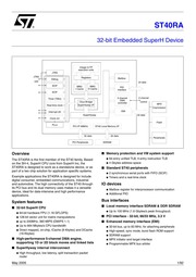
9. ST40RA 32 bit Embedded SuperH Device Integer amp FP execution units gt JTAG zs TA Debug registers Mailbox UDI 5 x 24 data TT Ser MMU MMU PIO Cache D Cache interface lt gt SCIF T Timer TMU X 7 5 channel 2 channel Cbus Bridge oM control controller MPX Real time clock SuperHyway I F Coprocessor gt LL Interrupt ctrl EMI SuperHyway 32 data Clockctrl M Flash 7 PCI I F 66MHz ST40 Local Memory I F 32 data 64 data M NZ NZ Peripherals PCI Peripherals SDRAM Overview The ST40RA is the first member of the ST40 family Based on the SH 4 SuperH CPU core from SuperH Inc the ST40RA is designed to work as a standalone device or as part of a two chip solution for application specific systems Example applications the ST40RA is designed for include digital consumer embedded communications industrial and automotive The high connectivity of the ST40 through its PCI bus and its dual memory uses makes it a versatile device ideal for data intensive and high performance applications System features B 32 bit SuperH CPU e 64 bit hardware FPU 1 16 GFLOPS e 128 bit vector unit for matrix manipulations e up to 200MHz 360 MIPS
10. 41 92 ST40RA 5 System configuration 5 9 6 3 SYSCONF SYS CON2 44 46 EMPI CS ENB Functional pin use and behavior Enable EMPI chip selection alternate function 000 NOTESCO remapped to NOTEMPICS 001 NOTESC1 remapped to NOTEMPICS 010 NOTESC2 remapped to NOTEMPICS 011 NOTESC3 remapped to NOTEMPICS 100 NOTESCA remapped to NOTEMPICS 101 NOTESC5 remapped to NOTEMPICS 110 Reserved 111 Disabled value at reset 0x0018 RW 47 SEL EXT EMI SLAVE 0 EMI is bus master 1 EMI is bus slave Select EMI slave or master functionality RW 48 59 Reserved 60 63 PIO CONF PIO CONF RW PIO alternate functions The function of pads with PIO alternate functions are controlled by the PIO PCO PIO PC1 and PIO PC2 registers In the ST40RA device the operational modes for these registers differ from the standard architecture definition and are shown in Table 15 Table 15 PIO alternate function registers PIO bit configuration PIO output state PIO PC2 PIO PC1 PIO PCO NonPIO function 7 0 0 0 PIO bidirectional Open drain 0 0 1 PIO output Push pull 0 1 0 PIO bidirectional Open drain 0 1 1 PIO input High impedance 1 0 0 PIO input High impedance 1 0 1 Reserved 1 1 0 Reserved 1 1 1 a State follovving reset 42 92 6 Clock generation ST40RA 5 9 7 PCI PERF register definition 6 1 43 92 PCI PERF 0
11. 5 9 4 2 SYSCONF SYS CON1 SYSCONF SYS CON1 Memory bridge control 0x010 3 0 Reserved RW 10 4 MB1 Memory bridge 1 control EMI target RW 17 11 MB2 Memory bridge 2 control EMPI initiator RW 24 18 MB3 Memory bridge 3 control EMI_SS target RW 38 25 Reserved 45 39 MB6 Memory bridge 6 control PCI initiator RW 52 46 MB7 Memory bridge 7 control PCI target RW 63 53 Reserved Where the two clocks are sourced from independent PLLs the bridge must be put in asynchronous mode 5 9 5 SYSCONF SYS CON2 SYSCONF SYS_CON2 Functional pin use and behavior 0x0018 The SYSCONF SYS CON register controls functional pin use and behavior LMI pad type RW 0 SSTL 8 LMI MODE 4 LVTTL Reset 0 Reference voltage source RW O internally generated reference voltage 1 external reference voltage from VREF pins Reset 0 9 LMILENVREF LMI control signal ECLK180 retime bypass RW 0 ECLK180 flip flop not bypassed 1 ECLK180 flip flop is bypassed Reset 0 10 LMI ECLK BYPASS Enable LMI 2 5 V compensation cell RW 0 LMI 2 5 V compensation cell enabled 1 LMI 2 5 V compensation cell disabled Reset 0 11 LMI NOTCOMP25 EN Enable LMI 3 3 V compensation cell RW 0 LMI 2 5 V compensation cell enabled 1 LMI 2 5 V compensation cell disabled Reset 0 12 LMI COMP33 EN 3 40 92 5 System configuration ST40RA 13 14 SYSCONF
12. DMIPS 1 1 e Up to 664 Mbytes s CPU bandwidth e Direct mapped on chip ICache 8 Kbytes and DCache 16 Kbytes B High performance 5 channel DMA engine supporting 1D or 2D block moves and linked lists B SuperHyway internal interconnect e High throughput low latency split transaction packet router May 2005 B Memory protection and VM system support e 64 entry unified TLB 4 entry instruction TLB e 4 Gbytes address space B Standard ST40 peripherals e 2 synchronous serial ports with FIFO SCIF e Timers and a real time clock IO devices e Mailbox register for interprocessor communication e Additional PIO Bus interfaces B Local memory interface SDRAM amp DDR SDRAM e Up to 100 MHz 1 6 Gbytes s peak throughput B PCI interface 32 bit 66 33 MHz 3 3 V B Enhanced memory interface EMI e 32 bit bus up to 83 MHz for attaching peripherals e High speed sync mode burst flash ROM support e SDRAM support e MPX initiator and target interface e Programmable MPX bus arbiter 1 92 ST40RA Appendix A Appendix B 3 A 1 A 1 1 A 1 2 A 1 3 A 1 4 A 1 5 A 1 6 A 2 A 2 1 A 2 2 A 2 3 A 2 4 A 2 5 B 1 B 1 1 B 1 2 B 1 3 B 1 4 B 2 B 2 1 B 2 2 B 2 3 B 2 4 B 2 5 B 3 B 3 1 B 3 2 B 3 3 B 4 B 4 1 B 5 B 5 1 B 5 2 Contents Interconnect architecture 0 ee ee eee 6 Arbitration SCHOMES 22 sa edit Paese ER ds he d a a ques OE EF 7 PCI arbiter C
13. LDATA44 H1 MD44 Memory data SL VO LDATA45 H2 MD45 Memory data SL VO LDATA46 G1 MD46 Memory data SL VO LDATA47 G2 MD47 Memory data SL VO LDATA48 T1 MD48 Memory data SL VO LDATA49 T2 MD49 Memory data SL VO LDATA50 R1 MD50 Memory data SL VO LDATA51 R2 MD51 Memory data SL 1 0 LDATA52 P1 MD52 Memory data SL 1 0 LDATA53 P2 MD53 Memory data SL 1 0 LDATA54 N1 MD54 Memory data SL 1 0 LDATA55 N2 MD55 Memory data SL VO LDATA56 Y1 MD56 Memory data SL 1 0 LDATA57 Y2 MD57 Memory data SL 1 0 LDATA58 Wi MD58 Memory data SL 1 0 LDATA59 W2 MD59 Memory data SL VO LDATA60 V1 MD60 Memory data SL VO LDATA61 V2 MD61 Memory data SL VO LDATA62 U1 MD62 Memory data SL VO LDATA63 U2 MD63 Memory data SL VO LBANKO J3 BAO Mem bank address SL O Table 38 PBGA ballout for STAORA 75 92 Ayy ST40RA 8 Pin description Pin function Pin Pin name Loc Sinai name Default Alternate Type Dir LBANK1 J4 BA1 Mem bank address SL O LADDRO G3 MAO Memory page column address SL O LADDR1 G4 MA1 Memory page column address SL O LADDR2 G5 MA2 Memory page column address SL O LADDR3 F3 MA3 Memory page column address SL O LADDR4 F4 MA4 Memory page column address SL O LADDR5 F5 MA5 Memory page column address SL O LADDR6 E3 MA6 Memory page column address SL O LADDR7 E4 MA7 Memory page column address SL O LADDR8 E5 MA8 Memory page column address SL O LADDR9 D
14. PIO input High impedance 1 0 1 Reserved 1 1 0 Reserved 1 1 1 a State follovving reset B 6 2 PCI PIO alternate functions The following PIO signals cannot be used when PCI is enabled even if the PCI implementation does not require the primary pin function Table 3 PCI PIO alternate functions BPN Pin function Pin Architecture Fin name signal name Row Col 9 Default Alternate Type Dir NOTPREQO E 18 NOTPCI_REQO PCI external request for bus PIO16 P8 VO VO NOTPREG1 E 17 NOTPCI_REQ1 PCI external request for bus PIO18 P8 VO NOTPREQ2 F 16 NOTPCI_REQ2 PCI external request for bus PIO20 P8 VO NOTPREG3 G 16 NOTPCI REQ3 PCI external request for bus PIO22 P8 I VO EMPIDREQ1 O If PCI is disabled the alternate functions may be used 3 17 92 ST40RA B Implementation restrictions B 7 B 7 1 B 7 2 B 7 3 B 8 B 8 1 B 8 2 B 8 3 3 Interconnect Memory bridge functionality Ensure there is no traffic passing though the memory bridge when changing frequency Semisynchronous modes of operation are not supported Clock selection The alternate CLOCKGENB clock is not supported for the LMI Pad drive control Programmable drive strength control is not supported for DDR operation GPDMA Linked list support Decrementing transfers are not supported as part of link list transfer sequences 2 D transfer
15. ST40RA 7 5 65 92 LMI interface DDR SDRAM AC specifications Figure 13 LMI DDR mode timings Inputs Outputs tLCHLCL tLCLLCH b LCHLCH dt gt NOTLCLKOUTA B a a LCLKOUTA B tLCLLAV LMIADDR COM ODO DQSH DQSL LCHDQSR LCHDQSR DOSREAD i tDQSRH DQSRH DQSRS LMIDATAREAD LCHDQS tpasH tos DOSWRITE 1 LMIDATAWRITE tLDWH tLCHDWZ DD Table 30 LMI DDR SDRAM AC timings Symbol Parameter Min Max Units Note tLCHLCH LMI clock period 10 ns tLCHLCL LMI clock high time 0 45 tLCHLC H ky ST40RA 7 Electrical specifications Table 30 LMI DDR SDRAM AC timings Symbol Parameter Min Max Units Note ti cLLCH LMI clock low period 0 45 L CHLCH L CHLAV LCLKOUT low to address and command 1 5 1 5 ns valid L CHDQSR LCLKOUT high to read DOS edge 1 5 1 5 ns a tDOSH DOS high 0 45 ti cHLCH DQSL DQS low 0 45 ti cHLCH tpasrs Read data setup for DQS edge 1 t cHLCH 4 ns a tposnH Read data hold for DQS edge ti CHLCH 441 ns a ti CHDQS LCLKOUT high to write DQS N ti cHLCH 4 N ti cHLCH ns 0 75 4 4 0 75 ti pws Write data setup to DQS edge N ti CHLCH 4 ns 0 75 ti pwH DQS edge to Write data invalid N ti cHLCH 14 ns 0 75 L CHDVVZ LCLKOUT high to vvrite data Z 2 ns
16. I EADDR17 U12 MA17 EMI external address MODE15 E4 O I EADDR18 U13 MA18 EMI external address MODE16 E4 O I EADDR19 U14 MA19 EMI external address MODE17 E4 O I EADDR20 V15 MA20 EMI external address MODE18 Es O I EADDR 1 U15 MA21 EMI external address MODE19 E4 O I EADDR22 T15 MA22 EMI external address E4 O EADDR23 V16 MA23 EMI external address E4 O EADDR24 U16 MA24 EMI external address E4 O EADDR25 T16 MA25 EMI external address EMPIDACK1 E4 O EADDR26 V17 MA26 EMI external address EMPIDACKO E4 O I EDATAO WA MDO External data MPX address E4 yo EDATA1 Y4 MD1 External data MPX address E4 VO EDATA2 W5 MD2 External data MPX address E4 VO EDATA3 Y5 MD3 External data MPX address E4 VO EDATA4 V6 MD4 External data MPX address E4 y o EDATAS W6 MD5 External data MPX address E4 VO EDATA6 Y6 MD6 External data MPX address E4 VO EDATA7 V7 MD7 External data MPX address E4 VO EDATA8 W7 MD8 External data MPX address E4 VO EDATA9 Y7 MD9 External data MPX address E4 VO EDATA10 V8 MD10 External data MPX address E4 y o EDATA11 wa MD11 External data MPX address E4 VO EDATA12 Y8 MD12 External data MPX address E4 VO EDATA13 V9 MD13 External data MPX address E4 y o EDATA14 Y9 MD14 External data MPX address E4 VO EDATA15 W9 MD15 External data MPX address E4 VO EDATA16 W11 MD16 External data MPX address E4 y o EDATA17 Y11 MD17 External data MPX address E4 VO EDATA18 W12 MD18 External data MPX address E4 VO Table 38 PBGA ballout for STAORA 81 92 Ay ST40R
17. PBGA package 20 19 18 17 16 15 14 13 12 11 10 9 8 7 6 5 4 3 2 1 A J x du OOOO 4 V OOO OOOO OOOO A ODODUCOOQQOUDOOOQOUOO B COORD OOO OOD OOO OO Uo B 2 OOOOOOOOOOOOOOOOOOO D 0000000000000 O 00 ODO ODO E 000000 OOOOOOOOOOOOOO F OUOCUQQ OOOQOQ G GOO OOGO OUOGOOQO H QODOOCO 000000 1000000 J _ OOOOOU ooo 000000 K ul Hn 000000 000000 OOOOO0 L 7 0000001 90001000 000000 M COO DOO 60000 000000 N OO F OO OO A OOO OO TOO OO y OOO OO h OOO iid v Y v 4 f Detall D_ Option 36 thermal balls ky 88 92 9 Package ST40RA 89 92 Figure 21 Package layout viewed through package A1 corner index area Seating plane Side view 3 ST40RA 9 Package Table 40 Package dimensions Dimensions Ref Databook mm Drawing mm Description Min Typical Max Min Typical Max A 2 6 2 6 Overall thickness A1 0 36 0 5 0 7 Ball height A2 1 9 1 63 1 9 Body thickness b 0 6 0 75 0 9 0 6 0 75 0 9 Ball diameter D 26 8 27 27 2 26 8 27 0 27 2 Body size D1 24 13 24 13 Ball footprint E 26 8 27 27 2 26 8 27 0 27 2 Body size E1 24 13 24 13 Ball footprint e 1 27 1 27 Ball pitch f 1 435 1 435 Ball to edge ddd 0 2 0 2 Co planarity eee 0 15 0 15 Cylindrical tolerance 3 fff 0 075 0 75 Cylindrical tolerance 4 ky 90 92 Revision history ST40RA 91 92 Revision history STMicroelectronics Date Revision Cha
18. STATUS1 0 O 11 O 11 00 AUDATAO 3 O 00 O 0000 AUDSYNC O 1 O 1 AUDCLK O 0 O 0 NOTASEBRK VO 1 DCLK TCK EADDR TDI I 0 NOTTRST I 0 1 TDO O Z O Z 3 86 92 8 Pin description ST40RA 87 92 Table 39 Pin reset states for ST40RA Architecturally defined Implementation reset state during and after pin ames reset state reset Dir During reset Dir During reset Following reset EMI system pins EADDR 2 26 O Z VO ZZZE740 0 Mode 0 EDATAJ 0 31 VO Z VO Z ECLKOUT MCLKOUT O 0 O 0 FCLKOUT ECLKEN Z O Z 1 EDQM 0 3 Z O Z 1111 NOTECS 0 5 1 VO Z 111111 NOTERAS NOTECAS VO 1 VO Z 1 NOTEWE EWAIT VO Z VO Z EPENDING O 0 MD7 0 VO Z 0 Z MD7 1 MD7 NOTMREQ I Z EMI HOLD ACK when EMI slave NOTMACK O Z O Z 1 EMI HOLD REQ when EMI slave NOTFBAA O Z O Z 1 NOTESCS 0 2 O Z VO Z a The reset state of the EADDR bus is tri state the value given corresponds to a specific boot mode and shows the expected ties q ST40RA 9 Package 9 Package Physical properties e 27 x27 mm 372 plastic ball grid array PBGA 336 36 thermal ground balls e Typical power consumption 2 W e Substrate height 0 56 mm e Total height 2 33 mm e Cover substrate 1 73 mm Figure 20 and Figure 21 are diagrams of the pin disposition on the package Figure 20 372 pin
19. STBACK mapping for modules CLOCKGENA CLOCKGENB Bit number mapping mapping 0 EMI Reserved 1 LMI Reserved 2 DMAC Reserved 3 PCI Reserved 4 PIO Reserved 5 Reserved Reserved 6 Reserved PCI bus 7 Reserved Reserved 55 92 ky ST40RA 7 Electrical specifications 7 7 1 Electrical specifications DC absolute maximum ratings Table 23 Absolute maximum ratings Symbol Parameter Min Max Units VDDCORE Core DC supply voltage 2 1 V VDDio VO DC supply voltage 4 0 V VDDRTC RTC DC supply voltage 2 1 V Vio Voltage on input output and bidirectional pins GND 0 6 VDDio 0 6 V VIORTC Voltage on input pins on VDDRTC supply GND 0 6 VDDRTC 0 6 V LPCLKIN LPCLKOSC VlOci Voltage on CLKIN and CLKOSC pins GND 0 6 VDDcoRE 0 6 V lo DC output current 25 mA Ts Storage temperature ambient 55 125 deg C TA Temperature under bias ambient 55 125 deg C Notes a Stresses greater than those listed under Table 23 Absolute maximum ratings may cause permanent damage to the device This is a stress rating only and functional operation of the device at these or any other conditions above those indicated in the operating sections of this specification is not implied Exposure to absolute maximum rating conditions for extended period may effect reliability b All VO pins are 3 3 V tolerant except CLKIN LPCLKIN CLKOSC and LPCLKOSC 7 1 1 Fmax clock domains Table 24 Fmax clock d
20. SYS_CON2 LMI_SDRAM_DATA_DRIVE Functional pin use and behavior SDRAM data and data strobe pad PROG 1 0 LVTTL OP drive strength 00 1x 01 2x 10 3x 11 4x Reset 0 0x0018 RW 15 16 LMI_SDRAM_ADD_DRIVE LMI address and control pad PROG 1 0 LVTTL OP drive strength 00 1x 01 2x 10 3x 11 4x Reset 0 RW 17 35 Reserved 36 EMPI ENB O Enable EMPI channel 0 DREQ DRACK DRACK alternate function 0 Disabled 1 NOTESCS1 remapped to EMPIDREQO NOTESCS2 remapped to EMPIDRAKO EADDR26 remapped to EMPIDACKO EADDR26 is only remapped when whilst the ST40RA is acting as a bus slave RW 37 38 EMPI ENB 1 EMPI_ENB 2 Enable EMPI channel 1 DREQ DRACK DRACK alternate function 0 Disabled 1 NOTPREQ3 remapped to EMPIDREQ1 NOTPGNT3 remapped to EMPIDRAK1 EADDR25 remapped to EMPIDACKO EADDR25 is only remapped when whilst the ST40RA is acting as a bus slave Enable EMPI channel 2 DREQ DRACK DRACK alternate function 0 Disabled 1 DREQO remapped to EMPIDREQ2 DACKO remapped to EMPIDACK2 DRAKO remapped to EMPIDRAK2 RW RW 39 40 EMPI_ENB 3 MAILBOX_ENB Enable EMPI channel 2 DREQ DRACK DRACK alternate function 0 Disabled 1 DREQ1 remapped to EMPIDREQ3 DACK1 remapped to EMPIDACK3 DRAK1 remapped to EMPIDRAK3 Enable mailbox interrupt alternate function 0 Disabled 1 NOTESCO remapped to MBXINT RW RW 41 43 Reserved
21. an external clock source may be used Type 2 configuration accesses Configuration space accesses to devices across a PCI bridge are implemented as type 2 operations on the PCI bus In this implementation such accesses must be broken into a sequence of byte operations For example access to a 32 bit register is through four single byte operations Software visible changes between STB1HC7 and ST40RAH8D PCI PLL reprogramming required for H7 parts is no longer required for H8 The PCI PLL register is renamed from PLLPCICR to CLKGENA PLL2CR The register implementation for PCI MBAR mappings has changed between the STB1HC7 and ST40RAH8D implementations and software device drivers should reflect this Error behavior The implementation of local PCI register error handling is not fully implemented 3 ST40RA B Implementation restrictions B 2 5 B 3 B 3 1 B 3 2 B 3 3 B 4 B 4 1 B 5 B 5 1 B 5 2 3 Master abort When operating as a bus master the PCI module is not guaranteed to have the value OXFFFF FFFF following a master abort of a read cycle The master abort may be detected using either the PCI module status and interrupt information supplied by the module EMI EMPI EMPI burst mode operation ST40RA MPX target MPX operations using the ST40RA as the target which lead to burst requests to memory Read ahead 8 16 and 32 byte read operations have limited support MPX operations from the ST40RA as
22. device is 8 16 or 32 bits wide The 16 bit bank must use EDQM3 as address 1 the LSB address for the device and the 8 bit bank must use EDQM3 as address 1 and EDOM as address 0 See the ST40 System Architecture Manual Volume 2 Bus Interfaces for details of setting the device type and port size using the EMI configuration registers Table 10 Mapping the internal address lines of a connected device Device type SDRAM Peripheral SFlash MPX Port size Device address 25 to 2 Device address 1 Device address 0 32 bit EADDR 25 2 16 bit EADDR 24 2 EDOM3 8 bit EADDR 23 2 EDQM3 EDQM2 EADDR 25 2 q ST40RA 5 System configuration 5 7 3 EMI pin to function relationship Table 11 EMI pin functions ST40RA EMI pin Peripheral SFlash SDRAM MPX MPX EMPI EADDR 2 26 MEM ADDRESS MEM ADDRESS MEM ADDRESS EADDR3 NOT_CS CLK CLK EADDR4 NOT_OE ICS ICS EADDR5 NOT BE FRAME FRAME EADDR6 MEM_DATA BS BS EADDR7 write ANE WE EADDR8 MEM DATA VO 31 0 VO 31 0 EADDR9 read VO 63 61 VO 63 61 EDATA 0 31 MEM DATA MEM DATA MEM DATA MEM DATA 31 0 MEM DATA 31 0 ECLKOUT SDRAMCLOCK ECLKEN CKEN EDQMO NOT BEO NOT BEO NOT MEMBEO EDOM 1 NOT BE1 NOT BE1 NOT MEMBE1 EDQM2 NOT BE2 NOT BE2 NOT MEMBE2 EDQM3 NOT_BE3 NOT_BE3 NOT_MEMBE3 NOTECSO NOT_CSO NOT_CSO NO
23. in this publication are subject to change without notice This publication supersedes and replaces all information previously supplied STMicroelectronics products are not authorized for use as critical components in life support devices or systems without express written approval of STMicroelectronics The ST logo is a registered trademark of STMicroelectronics All other names are the property of their respective owners 2005 STMicroelectronics All rights reserved STMicroelectronics group of companies Australia Belgium Brazil Canada China Czech Republic Finland France Germany Hong Kong India Israel Italy Japan Malaysia Malta Morocco Singapore Spain Sweden Switzerland United Kingdom United States of America www st com Ayy 92 92
24. only register is shown in Section 5 9 4 1 SYSCONFSYS STAT1 on page 39 Changing control of a memory bridge At reset all these bridges are set to be synchronous After reset and boot the function of these memory bridges can be changed See Section 5 9 4 SYSCONF registers on page 39 The procedure for changing the control of a memory bridge is given below 1 Ensure noinitiators are accessing the subsystem the bridge is connected to and ensure the subsystem cannot initiate any requests to the SuperHyway 2 Stop the clock to the subsystem 3 Change the memory bridge configuration using the SYS CONF SYS CON register as detailed in Table 13 4 Restart the clock to the subsystem and reinitialize the system 3 ST40RA 5 System configuration 5 9 System configuration registers Table 14 outlines the ST40RA system configuration registers Table 14 System configuration registers Address ee Register Module offset Type Description EMI GENCFG EMI 0x028 R W EMI general purpose configuration register see Section 5 9 1 EMI GENCFG EMI general configuration on page 37 LMI COC LMI 0x028 R W LMI clock and pad control register see Section 5 9 2 LMI COC on page 38 LMI CIC LMI 0x040 RO LMI clock and pad status see Section 5 9 3 LMI CIC on page 39 SYS_STAT1 SYSCONF 0x040 RO Memory bridge status see Section 5 9 4 1 SYSCONF SYS_STAT1 on page 39 SYSCONF SYS_CON1 SYSCONF 0x010 R W System configur
25. output signals valid 1 10 ns a b tPCIHAOZ PCLK high to all PCI outputs tri state 2 14 ns a tPCIHAON PCLK high to all PCI outputs on 2 ns a tBIVPCIH Bused input signals valid to PCLK high 3 ns c tPIVPCIH Point to point input signals valid to PCLK high 5 ns b tPCIHAIX All PCI input signals hold after PCLK high ns a Specified with 30 pF load b Need to use 4 ns of the PCI propagation delay c NOTPREQT0 3 and NOTPGNT 0 3 are point to point signals and have different input setup times to bussed signals All other synchronous signals are bussed 3 ST40RA 7 Electrical specifications 7 4 3 LMI interface SDRAM AC specifications Figure 12 LMI SDRAM mode timings tLCHLICH pn gt LCLKOUTA LCLKOUTB tLCHLCL tLCLLCH ml gt tLCLLOV 7 Outputs LCHLON LCHLOZ gt Tri state outputs LCHLIX tLIVLCH L 5 Inputs Table 29 LMI SDRAM AC timings Symbol Parameter Min Max Units Note tLCHLCH LMI clock period 10 ns tLCHLCL LMI clock high time 0 45 tLCHLCH tLCLLCH LMI clock low period 0 45 tLCHLCH tLCHLOV LCLKOUT low to output signals valid 2 2 ns tLCHLOZ LCLKOUT high to outputs tri state 0 2 ns tLCHLON LCLKOUT high to outputs on 2 ns tLIVLCH Input signals valid to LCLKOUT high 2 ns tLCHLIX Input signals hold after LCLKOUT high 2 ns 64 92 7 Electrical specifications
26. tene atd Web WENGER 47 CLOCKGENA 2x PCI PCI DIV BYPASS 0 48 Division ratios on CLOCKGENA 2x tees 48 Setting clock frequencies as ar EER RE rk a RE ER EE ERE TR ER Ri 49 Programming the PLL output frequency eee 50 Changing clock frequency eee eeen 50 Changing the core PLL frequencies enen eene eh 50 Changing the frequency division ratio eee eee 51 Power Management cesse xa A EE pk d ea 51 CPU low power modes ooo 51 Module low power modes eeen 51 Clock generation registers es wed em Rex beu EE ete eke ste ox Pee ed 51 CLOCKGENB CLK SELCR register 9 00 0000000 3 0 i ST40RA 6 6 2 CPG STBCR register eneen 53 6 6 3 CLOCKGENA STBREQCR and CLOCKGENB STBREQCR registers 54 6 6 4 CLOCKGENA STBREQCR SET and CLOCKGENB STBREQCR SET registers 54 6 6 5 CLOCKGENA STBREQCR CLR and CLOCKGENB STBREQCR CLR register 54 6 6 6 CLOCKGENA STBACKCR and CLOCKGENB STBACKCR register 55 Chapter 7 Electrical specifications eee 56 7 1 DC absolute maximum ratings ee ee ee ee ol de ee 56 7 1 1 Fmax clock doOmains zeit turn bidet hs ORR A ende TULLIA LEM BELA sad 56 7 1 2 Operating conditions s ne tr ee en en day tae ane al m b eM ews s 57 7 1 3 Pad specific output AC characteristics eee ee 58 7 2 Rise a
27. the total load on the CLOCKOSC output is 2pF Table 33 CLKIN timings Symbol Parameter Min Nom Max Units Notes tCLCH CLKIN pulse width low 6 ns tCHCL CLKIN pulse width high 6 ns tCLCL CLKIN period 27 MHz a tcr CLKIN rise time 10 ns b c CT CLKIN fall time 10 ns 2 3 a Measured betvveen corresponding points on consecutive falling edges b VVhen driven by an extermal clock c Clock transitions must be monotonic within the range VIH to VIL Figure 17 CLKIN timings VDDcone 0 8 VDDcone 0 5 3 69 92 ST40RA 7 Electrical specifications 7 10 3 Lovv povver CLKIN AC specifications The timings referenced in Figure 18 refer to the case where CLKIN is directly clocked from an external source In this case care should be taken that the total load on the LPCLKOSC output is 2pF Table 34 LPCLKIN timings Symbol Parameter Min Nom Max Units Notes tLCLLCL LPCLKIN period 32 678 kHz a b LPCLKIN duty cycle 10 50 90 tLCr LPCLKIN rise time 10 ns c d tLCf LPCLKIN fall time 10 ns 3 4 a Measured between corresponding points on consecutive falling edges b Variation of individual falling edges from their nominal times c When driven by an external clock Transitions must be monotonic within the range VIH to VIL o Figure 18 CLKIN timings VDDRrc 0 8 VDDgrc 0 5 VDDgrc 02 tLCLLCL
28. 0 70 C ST40RA166XH6 166 MHz 40 C 85 C ST40RA200XH6 200 MHz 40 C 85 C VDD Core 1 65V to 1 95V 1 80V to 1 95V 19 92 ky STAORA 4 Architecture 4 Architecture 4 1 Overview 4 2 4 2 1 The ST40RA combines an SH 4 32 bit microprocessor with a wide range of interfaces to external peripherals This section briefly describes each of the features of the STAORA ST40 system SuperH ST40 SH 4 core Figure 2 illustrates the system architecture of the ST40 SH 4 core The following section briefly describes the features and performance of the core Figure 2 ST40 SH 4 core architecture CPU UBC FPU 5 33 pe fo Za o lo 8 8 5 9 Is E B 5 IS 5 Lower 32 bit data 2 2 s s 2 S s s S S Bl 8 6 lo x el 5 BG S le el fo i 50 e x 9 x Lower 32 bit data i amp SLE IS 8 AF TESS ICache 8 Kbytes ITLB Cache and TLB UTLB DCache 16 Kbytes controller v Es b s 3 5 9 8 pun e amp 5 e A e 3 Central processing unit The central processing unit is built around a 32 bit RISC two way superscalar architecture Operating at 166 MHz it runs vvith high code density using fixed length 16 bit instructions lt has a load store architecture delayed branch instruction ca
29. 0800 0000 OxOEFF FFFF LMI control registers OXOFOO 0000 OxOFFF FFFF PCI 0x1000 0000 Ox16FF FFFF PCI control registers 0x1700 0000 Ox17FF FFFF Reserved 0x1800 0000 Ox1AFF FFFF ST40 core peripherals ST40 System Architecture Manual Volume 1 System DMAC 0x1B00 0000 0x1B00 FFFF PIO1 0x1B01 0000 0x1B01 FFFF PIO2 0x1B02 0000 0x1B02 FFFF PIO3 0x1B03 0000 0x1B03 FFFF CLOCKGEN 0x1B04 0000 0x1B04 FFFF Interconnect 0x1B05 0000 Ox1BO5 FFFF Reserved Ox1B06 0000 Ox1BOF FFFF CLOCKGENB Ox1B10 0000 0x1B10 FFFF Reserved 0x1B11 0000 Ox1B12 FFFF EMPI 0x1B13 0000 Ox1B13 7FFF ST40 System Architecture Manual Volume 2 Bus Interfaces MPXARB 0x1B13 8000 Ox1B13 FFFF ST40 System Architecture Manual Volume 2 Bus Interfaces ST40RA additional peripherals ST40 System Architecture Manual Volume 4 I O Devices MailBox 0x1B15 0000 0x1B15 FFFF SYSCONF 0x1B19 0000 0x1B19 FFFF Reserved 0x1B1A 0000 Ox1B1F FFFF Reserved for additional peripherals Reserved 0x1B20 0000 Ox1B3F FFFF ST40 core peripherals ST40 System Architecture Manual Volume 1 System INTC2 Ox1E08 0000 OX1EOF FFFF 26 92 5 System configuration ST40RA 5 2 27 92 Table 5 STAORA system address map Address Module Reference Base Top Reserved CPU only 0x1E10 0000 Ox1FBF FFFF registers CPG Ox1FC
30. 1 Bank 4 to 5 Reset 0 6 EWPU Pull up on EWAIT pin EN 0 Disabled 1 Enabled Reset 0 7 EAPU Pull up enable on EADDR pins RW 0 Disabled 1 Enabled Reset 0 31 8 Reserved 0 Ignored 1 Reserved Reset Undefined a If the EWAIT signal is set at the beginning of an access and the data is to be set after the EWAIT is cleared the parameters ACCESSTIMEREAD and LATCHPOINT in the EMI configuration registers must be set as follows ACCESSTIME LATCHPOINT 3 See the ST40 System Architecture Manual Volume 2 Bus Interfaces for details of setting the EMI configuration registers 3 37 92 ST40RA 5 System configuration 5 9 2 LMI COC LMI COC LMI clock and pad control 0x028 LMI COC allows modification of the glue logic 0 DLY_SRC Delay line control source RW 0 DLL provides delay line control 1 LMI CFG 5 1 provides delay line control Reset 0 5 1 DLY_NUM Number of delays 200ps each RW Reset 0 7 6 DLY_FRQ_RES External delay frequency resolution RW Reset 0 19 8 PLL_SETUP PLL setup RW Reset 0 21 20 DLL PRO CON DLL programmer control RW Reset 0 22 FRQ RES SRC Frequency resolution source of external delay RW 0 DLL provides frequency resolution 1 LMI CFG 7 6 provides frequency resolution Reset 0 23 PLL SETUP PLL setup RW Reset 0 24 DLL PRO SRC DLL programmer source RW 0 Delay programmer block provide
31. 14 EADDR16 MD14 PCI PCI bridge mode H Host L Satellite MODE15 EADDR17 MD15 PCI Reserved PCI select clock e H External L Internal MODE16 EADDR18 MD16 Reserved Tie high f MODE17 EADDR19 MD17 MODE18 EADDR20 MD18 MODE19 EADDR21 MD19 See CLOCKGEN chapter of the ST40 System Architecture Manual for details a b ST40RA is always the clock master providing EMI clocks to the system O d reserved for enable retiming stage on EMI padlogic See EMI chapter of the S740 System Architecture Manual for details e PCI clock is selected externally on the board for ST40RA The mode pin may be used for clock selection in future variants f These mode pins are not used in current variants however they may be used to enable additional functionality in future variants 3 ST40RA 8 Pin description 8 3 PBGA 27 x 27 ballout This should be used in conjunction with Figure 21 Package layout viewed through package on page 89 Architecture Pin function Pin gnal name Default Alternate Type Dir LDATAO A17 MDO Memory data SL VO LDATA1 B17 MD1 Memory data SL VO LDATA2 A18 MD2 Memory data SL VO LDATA3 B18 MD3 Memory data SL VO LDATA4 A19 MD4 Memory data SL VO LDATAS B19 MD5 Memory data SL VO LDATA6 A20 MD6 Memory data SL VO LDATA7 B20 MD7 Memory data SL VO LDATA8 A13 MD8 Memory data SL VO LDATA9 B13
32. 15 VDDCORE VDDLMI K5 VDDLMI VDDLMI F6 VDDLMI VDDLMI G6 VDDLMI VDDIO H6 VDDIO Table 38 PBGA ballout for ST40RA 83 92 Ayy ST40RA 8 Pin description Pin function Pin Pin name Loc ln Default Alternate Type Dir VDDLMI J6 VDDLMI VDDIO K6 VDDIO VDDLMI L6 VDDLMI VDDIO F7 VDDIO VDDLMI F8 VDDLMI VDDIO F9 VDDIO VDDIO E10 VDDIO VDDLMI F10 VDDLMI VDDIO F11 VDDIO VDDIO F12 VDDIO VDDIO F13 VDDIO VDDLMI F14 VDDLMI VDDLMI F15 VDDLMI VDDIO G15 VDDIO VDDIO H15 VDDIO VDDIO J15 VDDIO VDDIO K15 VDDIO VDDIO L15 VDDIO VDDIO L16 VDDIO 3 Table 38 PBGA ballout for ST40RA 84 92 8 Pin description ST40RA 8 4 Pin states The following table shows the direction and state of the pins during and immediately after reset e Z indicates an output or VO pin that has been tri stated e indicates an input or I O pin in input modes I O buffer tri stated e 1 indicates an output or I O pin driving logical high e O indicates an output or I O pin driving logical low e Xindicates an output or I O pin driving undefined data e Hindicates a pin with weak internal pull up enabled e Lindicates a pin with weak internal pull down enabled Table 39 Pin reset states for ST40RA Architecturally defined Implementation reset state during and after bit m s reset state rese
33. 16 FOWEF DWlkasas dann EE OR OE beads TO ee ase ax EE Qe 16 Module power down sequencing LLL L m rh 16 Accesses to modules in power down state eee 16 ST40RA B 6 B 6 1 B 6 2 B 7 B 7 1 B 7 2 B 7 3 B 8 B 8 1 B 8 2 B 8 3 Chapter 1 Chapter 2 Chapter 3 Chapter 4 4 1 4 2 4 2 1 4 2 2 4 2 3 4 3 4 3 1 4 3 2 4 3 3 4 4 4 4 1 4 5 4 5 1 4 5 2 Chapter 5 5 1 3 92 ale EE IE hse races vd eb E N ad a ep ROLE A D edd 17 PIO default functionality following reset Ie 17 PCI PIO alternate functions lll m mr 17 HETFC HR CE sa ab Bins a a quer Gs dat bi e etit ues 18 Memory bridge functionality EE EE ee Ee ee ek ee I nh 18 Glock selectlon t sa e evt ta edie dee ed e dee duct e eet ere 18 Pad drive control ee lh hh 18 GEDMA unta tara BAE RER B de Narie aia 18 Linked list support omt bas gta A DEERE RE Vee tinea re eno ts 18 2 D tf h f f ag ssp da sd jaa i es g p ts i r D v 18 Protocol si n lS sies tarn wanden Ea dien eX Lx rat edes 18 Scope of this document ses Boe oe ME ewe eked handed ELIT tee Es 19 ST40 documentation suite 19 CPU documenta Eran id erectis iio dee BR fast 19 System documentalloh sss i sr ED ER RR DE PERD ER EU Exe are C P ce CR 19 STAORA devices visas ike HR A Y E
34. 3 MA9 Memory page column address SL O LADDR10 D4 MA10 Memory page column address SL O LADDR11 D5 MA11 Memory page column address SL O LADDR12 C3 MA12 Memory page column address SL O LADDR13 C4 MA13 Memory page column address SL O LADDR14 C5 MA14 Memory page column address SL O LDQSO C19 DQSO DDR data strobe SL O LDQS1 B12 DQS1 DDR data strobe SL O LDQS2 A11 DQS2 DDR data strobe SL O LDQS3 B2 DQS3 DDR data strobe SL O LDQS4 B1 DQS4 DDR data strobe SL O LDQS5 L2 DQS5 DDR data strobe SL O LDGS6 M1 DQS6 DDR data strobe SL O LDQS7 W3 DQS7 DDR data strobe SL O LCLKOUTA D8 MCLKOA SDRAM clock output SL O NOTLCLKOUTA D7 NOTMCLKOA SDRAM clock output SL O LCLKOUTB L3 MCLKOB SDRAM clock output SL O NOTLCLKOUTB M3 NOTMCLKOB SDRAM clock output SL O LVREF H5 VREF DDR reference voltage I LDOMO C20 DQMO SDRAM data mask SL O LDQM1 A12 DQM1 SDRAM data mask SL O LDQM2 B11 DQM2 SDRAM data mask SL O LDQM3 A2 DQM3 SDRAM data mask SL O LDQM4 Al DQM4 SDRAM data mask SL O ky Table 38 PBGA ballout for ST40RA 76 92 8 Pin description ST40RA Pin function Pin Pin name Loc alu Default Alternate Type Dir LDQM5 L1 DQM5 SDRAM data mask SL O LDQM6 M2 DQM6 SDRAM data mask SL O LDQM7 YS DQM7 SDRAM data mask SL O NOTLCSAO C9 NOTCSAO Chip select A SL O NOTLCSA1 D9 NOTCSA1 Chip select A SL O NOTLCSBO H3
35. A 8 Pin description Pin function Pin Pin name Loc alu Default Alternate Type Dir EDATA19 Y12 MD19 External data MPX address E4 VO EDATA20 V13 MD20 External data MPX address E4 VO EDATA21 W13 MD21 External data MPX address E4 VO EDATA22 Y13 MD22 External data MPX address E4 VO EDATA23 V14 MD23 External data MPX address E4 VO EDATA24 W14 MD24 External data MPX address E4 VO EDATA25 Y14 MD25 External data MPX address E4 VO EDATA26 W15 MD26 External data MPX address E4 VO EDATA27 Y15 MD27 External data MPX address E4 VO EDATA28 W16 MD28 External data MPX address E4 VO EDATA29 Y16 MD29 External data MPX address E4 y o EDATA30 W17 MD30 External data MPX address E4 VO EDATA31 Y17 MD31 External data MPX address E4 1 0 ECLKOUT W10 ECLKOUT External clock for SDRAM O ECLKEN U10 ECLKEN External clock enable O EDQMO N4 EBE DOMO External byte enables VO EDQM1 P4 EBE DQM1 External byte enables VO EDQM2 P5 EBE_DQM2 External byte enables VO EDQM3 R5 EBE_DQM3 External byte enables VO NOTECSO R4 NOTECS5 External chip select One NOTECS 0 5 E4 O NOTECS1 T4 NOTECS4 External chip select 7 E4 O NOTECS2 T5 NOTECS3 External chip select Selected via E4 O software NOTECS3 T12 NOTECS2 External chip select E4 O NOTECS4 T13 NOTECS1 External chip select E4 O NOTECS5 T14 NOTECSO External chip select E4 O N
36. C16 AUDATA2 AUD bus command and data O AUDATA3 C15 AUDATA3 AUD bus command and data O AUDSYNC D15 AUDSYNC AUD command valid O AUDCLK D19 AUDCK AUD clock output O NOTASEBRK E9 NOTASEBRK Dedicated emulator pin C4 VO BRKACK DCLK D11 DCK Clock for udi TCK D12 TCK Test clock I TMS D10 TMS Test mode I NOTTRST E7 TRST Test reset I TDI E6 TDI Test data input I TDO E8 TDO Test data output O EADDR2 V4 MA2 EMI external address MODEO E4 O EADDR3 U4 MA3 EMI external address MODE1 E4 O EADDR4 V5 MA4 EMI external address MODE2 E4 O EADDR5 U5 MA5 EMI external address MODES E4 O I EADDR6 U6 MA6 EMI external address MODE4 E4 O EADDR7 T6 MA7 EMI external address MODE5 E4 O EADDR8 U7 MA8 EMI external address MODE6 E4 O EADDR9 T7 MA9 EMI external address MODE7 E4 O EADDR10 U8 MA10 EMI external address MODES E4 O I EADDR11 T8 MA11 EMI external address MODE9 E4 O ky Table 38 PBGA ballout for ST40RA 80 92 8 Pin description ST40RA Pin function Pin Pin name Loc HERE Default Alternate Type Dir EADDR12 U9 MA12 EMI external address MODE10 E4 O I EADDR13 T9 MA13 EMI external address MODE11 E4 O I EADDR14 V11 MA14 EMI external address MODE12 E4 O I EADDR15 U11 MA15 EMI external address MODE13 E4 O I EADDR16 V12 MA16 EMI external address MODE14 E4 O
37. CLK CLK CLK CLK Recommended reset configuration 0 200 100 50 25 50 50 50 Alternate reset configuration 1 266 133 88 44 88 88 88 2 300 150 100 50 100 100 100 3 332 166 111 66 111 111 111 Recommended operating modes 2 300 150 100 100 100 100 100 3 332 166 83 83 83 83 83 Low power configuration with clocks enabled programmable after reset A6 27 13 5 6 75 6 75 6 75 6 75 6 75 bypass 6 3 Clocks and registers at start up Reset Reset CLOCKGENA 20000 CLK1 CLK2 CLK3 CLK4 mede mode PLL1CR1 frequency fpi 2 CPU STBUS PER LMI MODE 2 0 reset value PLL1 CLK CLK CLK CLK 0 000 0x7939 8612 200 MHz 100 1 1 2 1 4 1 2 1 001 0x7939 B112 266 MHz 133 1 2 3 1 3 2 3 2 010 0x7938 6412 300 MHz 150 1 2 3 1 8 2 3 3 011 0x7938 7B14 332 MHz 166 1 2 3 1 3 2 3 4 100 0x7938 8612 400 MHz 200 1 1 2 1 4 1 2 5 101 0x7938 A712 500 MHz 250 1 1 2 1 4 1 2 6 110 0x0938 0000 0 MHz 0 1 1 2 1 2 1 2 i 111 0x0939 8612 200 MHz 100 1 2 1 4 1 4 1 4 Table 18 CLOCKGENA PLL1 reset values 47 92 r ST40RA 6 Clock generation 6 3 1 CLOCKGENA 2x PCI PCI DIV BYPASS 0 Table 19 CLOCKGENA PLL2 reset values PCI DIV BYPASS 0 Reset mode Reset value PLL2 frequency MODE 4 3 00 0x7938 B012 528 MHz 01 0x7938 B012 528 MHz 10 0x7938 B012 528 MHz 11 0x0938 B012 0 MHz 6 3 2 Division ratios on CLOCKGENA 2x Table 20 CLOCKGENA PLL2 PCI reset division ratios is Divide ratio selected
38. CTS1 PIO 0 7 2 x SCIF RXDO RXD1 SCKO SCK1 TXDO TXD1 8 2 Mode selection During the power on reset cycle a range of basic system configurations can be set up with resistive pull ups or pull downs A detailed description of these selections is found in the relevant chapters of the ST40 System Architecture Manual See Section 8 3 PBGA 27 x 27 ballout on page 74for information on which pins these mode inputs have been placed on the ST40RA Table 37 Mode selection pins for ST40RA Mode Architecture Block Pin name Description Notes pin signal name affected MODE2 0 EADDR2 MD2 0 CLOCKGEN Set system clock operating mode a EADDR3 EADDR4 MODE4 3 EADDR5 MD4 3 CLOCKGEN Set PCI clock operating mode 1 EADDR6 MODES EADDR7 MD5 CLOCKGEN Set clock input source H Crystal L External MODE6 EADDR8 MD6 CLOCKGEN Set enable CKIO ky 72 92 8 Pin description ST40RA 73 92 Table 37 Mode selection pins for ST40RA Mode Pin name 20116 77 Description Notes pin signal name affected MODE7 EADDR9 MD7 EMISS Enable MPX arbiter MODE8 EADDR10 MD8 System Set endianness H Little L Big MODE9 EADDR11 MD9 EMI Set EMI port b H Master L Slave MODE11 EADDR12 MD11 10 EMI Set booting ROM bus size 10 EADDR13 00 Reserved 01 32 bit 10 16 bit 11 8 bit MODE12 EADDR14 MD12 EMI Enable NOP when accessing flash c MODE13 EADDR15 MD13 Reserved Tie high d MODE
39. ECHEON EMI reference clock high to outputs on ns 1 tEIVECH Input signals valid to EMI reference clock high 4 ns b tECHEIX Input signals hold after EMI reference clock high 2 ns 2 a EMI reference clock is defined as the time when ECLKOUT MCLKOUT and FCLKOUT are all valid b Including EWAIT signal 3 ST40RA 7 Electrical specifications 7 8 PIO AC specifications Reference clock in this case means the last transition of any PIO output signal within a bus and hence is a virtual clock Table 32 PIO timings PIO13 0 PIO23 14 Symbol Parameter Units Note Min Max Min Max PCHPOV PIO reference clock high to PIO output valid 5 5 1 5 5 1 ns a PCHVVDZ PIO tri state after PIO reference clock high 5 5 5 5 ns 1 tPIOr Output rise time 1 5 1 5 ns tpior Output fall time 1 5 1 5 ns tpior Input rise time 20 5 ns b tpior Input fall time 20 5 ns 2 a No skew guarantee is made between the two separate PIO buses PIO13 0 and PIO23 14 b Loose input rise and fall times on PIO13 0 bus as these are schmitt trigger inputs Figure 16 PIO AC timings PIO reference clock gt 55 PCHPOV PCHVVDZ el ky 68 92 7 Electrical specifications ST40RA 7 9 System CLKIN AC specifications The timings referenced in Figure 17 refer to the case where CLKIN is directly clocked from an external source In this case care should be taken that
40. I arbiter and clock generator is provided inside the ST40RA For details on the configuration options for the PCI interface please see ST40 System Architecture Manual Volume 2 Bus Interfaces EMI MPX interface The EMI MPX interface contains the following blocks For full details of the configuration options of the EMI please see the S740 System Architecture Manual Volume 2 Bus Interfaces EMI memory interface initiator The EMI provides access to ROMs SDRAM memory mapped asynchronous external peripherals and synchronous MPX bus peripherals The EMI supports burst mode flash ROM and MPX for memory mapped device coupling The ST40RA GPDMA unit accesses external devices and two sets of DMA channels control signals are provided for this purpose EMPI memory interface target The EMPI is a synchronous MPX target that allows for an external MPX initiator to access the ST40RA internal memory space The EMPI contains a general purpose control channel and four high performance channels each of which implements a write buffer and a pair of 32 byte read ahead buffers able to optimize external device burst access to and from the ST40RA internal memory These buffers can be associated with memory regions within the ST40RA and external DMA channels Four sets of DMA handshake signals are provided to the EMPI to optimize long burst transfers between the ST40RA and external initiators like the STi5514 MPX bus arbiter The ST40RA has an internal progra
41. IF2 ERI 0x700 RXI 0x720 ih Oto 15 0 IPRC 7 4 to BRI 0x740 low TXI 0x760 WDT ITI 0x560 0 to 15 0 IPRB 15 12 ST40 standard system interrupt allocation Standard ST40 family interrupts are mapped as shown in Table 7 Table 7 ST40 standard interrupt allocation INTEVT Interrupt priority IPR Priority Interrupt source within IPR code nu bit numbers Value Initial value setting unit PCI PCI SERR INT OxA00 High to low PCI_ERR_INT OxA20 INTPRIOO O 3 High PCI AD INT OxA40 Oto 15 0 82 1 INTPRIOO 7 4 t PCI_PWR_DWN OxA60 low Reserved DMAC DMA_INTO OxB00 DMA_INT1 OxB20 DMA INT2 OxB40 High DMA INT3 OxB60 01015 0 INTPRIOO 1 1 8 to DMA_INT4 0xB80 low Reserved DMA ERR OxBCO PIOO PIOO OxC00 0 to 15 0 INTPRIOO 15 12 PIO1 PIO1 0xC80 Oto 15 0 INTPRIOO 19 16 PIO2 PIO2 OxDOO 0 to 15 0 INTPRIOO 23 20 3 ST40RA 5 System configuration 5 3 3 ST40RA VO device interrupt allocation Table 8 Mailbox and EMPI interrupt allocation INTEVT Interrupt priority IPR Priority Interrupt source E within IPR code bit numbers Value Initial value setting unit Mailbox MAILBOX 0x1000 Oto 15 0 INTPRIOA 0 3 High to low Reserved Reserved Oto 15 0 INTPRIO4 27 24 High to low EMPI INV ADDR 0x1380 0 to 15 0 INTPRI04 31 28 High to low Reserved 5 4 GPDMA channel mapping For full details of the GPDMA controller see S740 System Architecture Manual Volume 1 S
42. If CLOCKGEN A12 is used then the bridges may be placed in bypass mode This is the recommended mode of operation If either CLOCKGEN_B12 or CLOCKGEN A14 are used as the EMI CLK the memory bridges 1 2 and 3 must be enabled If CLOCKGEN A12 is used then the bridges may be placed in bypass This is the recommended mode of operation See Chapter 5 8 Memory bridge control on page 34 3 ST40RA 6 Clock generation Figure 6 ST40RA CLOCKGEN subsystem ST40RA ST40RA CLOCKGEN subsystem ST40 CLOCKGENA CLOCKCON Control ur vu SuperHyvvay v Control PLL2 ST40 CLOCKGENB 0 CPU CLK X ICK STBUS CLK X BCK gt PER CLK X PCK PCI BUS CLK external PCI SS CLK EMI SS CLK 11 EMI SEL 1 1 LMI SEL Contro Control pd CLK SEL 3 0 LMI CLK 3 46 92 6 Clock generation ST40RA 6 2 Recommended operating modes Table 17 Supported operating frequencies Mode for PLL CLOCKGENA and frequency ST40RA clock domain frequencies MHz CLOCKGENB MHz PLLA PLLB PLLA PLLB CPU STBUS _ PER LMI EMI SS PCI SS mode mode CLK CLK
43. MD9 Memory data SL VO LDATA10 A14 MD10 Memory data SL VO LDATA11 B14 MD11 Memory data SL 1 0 LDATA12 A15 MD12 Memory data SL 1 0 LDATA13 B15 MD13 Memory data SL 1 0 LDATA14 A16 MD14 Memory data SL 1 0 LDATA15 B16 MD15 Memory data SL VO LDATA16 A7 MD16 Memory data SL VO LDATA17 B7 MD17 Memory data SL VO LDATA18 A8 MD18 Memory data SL VO LDATA19 B8 MD19 Memory data SL VO LDATA20 A9 MD20 Memory data SL VO LDATA21 B9 MD21 Memory data SL 1 0 LDATA22 A10 MD22 Memory data SL VO LDATA23 B10 MD23 Memory data SL VO LDATA24 A3 MD24 Memory data SL VO LDATA25 B3 MD25 Memory data SL VO LDATA26 A4 MD26 Memory data SL VO LDATA27 B4 MD27 Memory data SL VO LDATA28 A5 MD28 Memory data SL VO LDATA29 B5 MD29 Memory data SL VO LDATA30 A6 MD30 Memory data SL VO ky Table 38 PBGA ballout for ST40RA 74 92 8 Pin description ST40RA Pin function Pin Pin name Loc alu Default Alternate Type Dir LDATA31 B6 MD31 Memory data SL VO LDATA32 F1 MD32 Memory data SL VO LDATA33 F2 MD33 Memory data SL VO LDATA34 E1 MD34 Memory data SL VO LDATA35 E2 MD35 Memory data SL VO LDATA36 D1 MD36 Memory data SL VO LDATA37 D2 MD37 Memory data SL VO LDATA38 C1 MD38 Memory data SL VO LDATA39 C2 MD39 Memory data SL VO LDATA40 K1 MD40 Memory data SL VO LDATA41 K2 MD41 Memory data SL VO LDATA42 J1 MD42 Memory data SL VO LDATA43 J2 MD43 Memory data SL VO
44. NOTCSBO Chip select B SL O NOTLCSB1 H4 NOTCSB1 Chip select B SL O NOTLRASA C8 NOTRASA Row add strobe A SL O NOTLRASB K4 NOTRASB Row add strobe B SL O NOTLCASA C7 NOTCASA Column add strobe A SL O NOTLCASB L4 NOTCASB Column add strobe B SL O NOTLWEA D6 NOTWEA Write enable A SL O NOTLWEB J5 NOTWEB Write enable B SL O LCLKENO C6 CKEO Clock enable SL O LCLKEN1 K3 CKE1 Clock enable SL O PADO T17 PCI_ADO PCI address and data P8 VO PAD1 T18 PCI AD1 PCI address and data P8 VO PAD2 R19 PCI AD2 PCI address and data P8 VO PAD3 R20 PCI AD3 PCI address and data P8 VO PAD4 R17 PCI AD4 PCI address and data P8 VO PAD5 R18 PCI AD5 PCI address and data P8 VO PAD6 P19 PCI_AD6 PCI address and data P8 VO PAD7 P20 PCI AD7 PCI address and data P8 VO PAD8 P17 PCI_AD8 PCI address and data P8 VO PAD9 P18 PCI AD9 PCI address and data P8 VO PAD10 N19 PCI AD10 PCI address and data P8 VO PAD11 N20 PCI AD11 PCI address and data P8 VO PAD12 N17 PCI AD12 PCI address and data P8 VO PAD13 N18 1 PCI AD13 PCI address and data P8 VO PAD14 M19 PCI AD14 PCI address and data P8 VO PAD15 M20 PCI AD15 PCI address and data P8 VO PAD16 K17 PCI AD16 PCI address and data P8 VO PAD17 K18 PCI AD17 PCI address and data P8 VO PAD18 J19 PCI AD18 PCI address and data P8 VO Table 38 PBGA ballout for STAORA 77 92 r ST40RA 8 Pin description Pin function Pi
45. O 0000 Ox1FC7 9999 RTC Ox1FC8 0000 Ox1FCF FFFF INTC OX1FDO 0000 Ox1FD7 9999 TMU Ox1FD8 0000 Ox1FDF FFFF SCIF1 OX1FEO 0000 Ox1FE7 9999 SCIF2 OX1FE8 0000 Ox1FEF FFFF EMU 0x1FFO 0000 OX1FF7 9999 Reserved Ox1FF8 0000 OX1FFF FFFF a For information about which address region to access for each module see SH 4 32 bit CPU Core Architecture sections 2 5 and 3 4 When operating in privilege mode these registers should be accessed via the P2 region by adding an offset of OxA000 0000 when operating in user mode access should be via the UO address System identifiers e SH 4 core processor identity 0x0100 e SH 4 core processor version 0x0541D e ST40RA HC8 TAP identity 05141041 e ST40RA HC8 PCI identity gt Vendor 104A Device 4000 gt gt gt gt Subsystem ID Revision ID 0x01 Class 0x4 0000 0x0000 3 ST40RA 5 System configuration 5 3 Note 5 3 1 3 Interrupt mapping For full details on the interrupt controller see ST40 System Architecture Manual Volume 1 System The mapping of the CPU interrupts is described in Section 5 3 1 Section 5 3 2 and Section 5 3 3 Some INTEVT codes are shown as reserved in Table 6 and therefore cannot be generated by this device ST40 core interrupt allocation The allocation of core interrupts is as shown in Table 6 Table 6 ST40 core interrupt allocation page 1 of 2
46. O Y19 RXDO PIO1 SCI receive data input PIO1 C2A VO RXD1 W20 RXD1 PIO4 SCI receive data input PIO4 C2A VO SCKO Y18 SCKO PIOO SCI clock input PIOO C2A VO SCK1 W18 SCK1 PIO3 SCI clock input PIOS C2A VO TXDO Y20 TXDO PIO2 SCI transmit data output PIO2 C2A O VO TXD1 W19 TXD1 PIO5 SCI transmit data output PIO5 C2A O VO NOTRST E14 NOTRESET Power on reset I IRLO C10 IRLO Interrupt request signal I IRL1 C11 IRL1 Interrupt reguest signal IRL2 C12 IRL2 Interrupt request signal IRL3 D13 IRL3 Interrupt request signal NMI C13 NMI Nonmaskable interrupt I Table 38 PBGA ballout for STAORA 79 92 ky ST40RA 8 Pin description Pin function Pin Pin name Loc aln Default Alternate Type Dir TMUCLK E15 1 TCLK RTC output clock TMU input clock C B VO VO LPCLKIN E12 EXTAL2 RTC crystal resonator input on VDDRrc supply LPCLKOSC E13 XTAL2 RTC crystal resonator output on VDDrrc supply O VDDRTC E11 VCCRTC Real time clock supply I CLKIN E20 CLKIN System clock input on VDDcoRe supply I CLKOSC D20 CLKOSC Crystal resonator pin on VDDcore supply O AUXCLKOUT E19 CKIO Reference 27 MHz clock O output STATUSO C14 STATUSO Processor operating status O STATUS1 D14 STATUS1 Processor operating status O AUDATAO C18 AUDATAO AUD bus command and data O AUDATA1 C17 AUDATA1 AUD bus command and data O AUDATA2
47. OTERAS U3 NOTERAS External raw add strobe MSTART and E4 O y o FLBADDR NOTECAS T3 NOTECAS External column address strobe MFRAME E4 O VO MPX FRAME and EOE N EMI output enable signal EWAIT T10 EWAIT External wait command E4 VO notready NOTEWE V3 NOTEWR External read not write E4 VO EPENDING NS EPENDING EMI pending refresh or access E4 O MCLKOUT Y10 MCLKOUT MPX clock O Table 38 PBGA ballout for ST40RA r 82 92 8 Pin description ST40RA Pin function Pin Pin name Loc alu Default Alternate Type Dir NOTMREQ R3 EMI BUS REQ or MPX bus request VO EMI HOLD ACK when EMI slave NOTMACK P3 EMI_BUS_GRANT MPX bus acknowledge VO or EMI HOLD REQ when EMI slave FCLKOUT V10 FCLKOUT Flash clock O NOTFBAA N5 Flash bus address advance O NOTESCSO L5 Reserved tri state MBXINT P8 O NOTESCS1 M5 Reserved tri state EMPIDREGO P8 O NOTESCS2 M4 Reserved tri state EMPIDRAKO P8 GND H8 N 36 ball array for ground supply and heat dissipation 13 VDDCORE M6 VDDCORE VDDCORE N6 VDDCORE VDDCORE P6 VDDCORE VDDCORE R6 VDDCORE VDDCORE R7 VDDCORE VDDCORE R8 VDDCORE VDDCORE R9 VDDCORE VDDCORE R10 VDDCORE VDDCORE R11 VDDCORE VDDCORE T11 VDDCORE VDDCORE R12 VDDCORE VDDCORE R13 VDDCORE VDDCORE R14 VDDCORE VDDCORE M15 VDDCORE VDDCORE N15 VDDCORE VDDCORE P15 VDDCORE VDDCORE R
48. OTPCI_REQO PCI external request for bus PIO16 P8 VO VO NOTPREO1 E17 NOTPCI_REQ1 PCI external request for bus PIO18 P8 VO NOTPREQ2 F16 NOTPCI REQ2 PCI external request for bus PIO20 P8 VO Table 38 PBGA ballout for STAORA Ayy 78 92 8 Pin description ST40RA Pin function Pin Architecture Pin name Loc siqnalam 9 Default Alternate Type Dir NOTPREQ3 G16 NOTPCI_REQ3 PCI external request for bus PIO22 P8 VO EMPIDREQ1 O NOTPGNTO D18 NOTPCI GNTO PCI grant external request PIO17 P8 VO VO NOTPGNT1 D17 NOTPCI_GNT1 PCI grant external request PIO19 P8 VO NOTPGNT2 E16 NOTPCI_GNT2 PCI grant external request P1021 P8 VO NOTPGNT3 D16 NOTPCI GNT3 PCI grant external request PIO23 P8 O VO EMPIDRAK1 PCLKOUT F20 PCI CLOCKOUT PCI clock output PIO14 P8 O VO NOTPINTA T19 NOTPCI INTA PCI interrupt request PIO15 P8 VO VO DACKO U19 DACKO DMA bus acknowledge PIO10 C2A O 1 0 EMPIDACK2 DRAKO U18 DRACKO DMA reguest acknowledge PIO9 C2A O VO EMPIDRAK2 DREQO V20 DREQO DMA transfer request PIO8 C2A I VO EMPIDREQ2 O DACK1 U20 DACK1 DMA bus acknowledge PIO13 C2A O 1 0 EMPIDACK3 DRAK1 T20 DRACK1 DMA reguest acknowledge PIO12 C2A O VO EMPIDRAK3 DREG1 U17 DREQ1 DMA transfer request PIO11 C2A I VO EMPIDREQ3 O SCI2 V19 RTS1 PIO7 SCI2 transmission request PIO7 C2A VO CTS1 V18 CTS1 PIO6 SCI2 transmission enabled PIO6 C2A O VO RXD
49. PCI PCI master request although not expected get served to avoid deadlock The priority orders have to be programmable and the latency checking algorithm can be enabled for GPDMA PCI EMPI EMI arbiter CPU buffer GPDMA PCI EMPI The default configuration after reset for fixed priority mode has to be in the following priority order e CPU buffer e PCI e EMPI e GPDMA The priority order have to be programmable and the latency checking algorithm can be enabled for GPDMA PCI EMPI LMI 1 arbiter CPU GPDMA PCI EMPI The default configuration after reset as to be to work fixed priority mode in the following priority order e CPU e GPDMA and PCI buffer The priority orders have to be programmable and the latency checking algorithm can be enabled for GPDMA PCI EMPI PER arbiter CPU GPDMA PCI EMPI The default configuration after reset as to be to work fixed priority mode in the following priority order e CPU buffer e PCI e EMPI e GPDMA The priority order have to be programmable and the latency checking algorithm can be enabled for GPDMA PCI EMPI q ST40RA A Interconnect architecture A 1 5 LMI2 arbiter CPU GPDMA PCI EMPI The default configuration after reset as to be to work fixed priority mode in the following priority A 1 6 A 2 3 order e PCI e EMPI e GPDMA e CPU buffer although the CPU requests are not supposed to go in that node to be send
50. PU GPDMA PCI EMPI eee 7 EMI arbiter CPU buffer GPDMA PCI EMPI RR II 7 LMI 1 arbiter CPU GPDMA PCI EMPI aaa 7 PER arbiter CPU GPDMA PCI EMP 9900000000 mu 7 LMI2 arbiter CPU GPDMA PCI EMPI 9900000 s 8 Return arbitration nan rie 757 8 Inierconn ci TegIbIGrS s uua ES EER KD RUE UR Ra Race e uA REOR EE eb See A RO RU E UR KORR E 8 BILE PI 9 H oo 10 EMI arbiter 11 ze Eu TT 12 Peripheral arbiter hr m 13 Implementation restrictionS 15 5150 Fi rer 15 EER zer RED E 15 Store queue povver dovvy rhe 15 giz dol olo 15 System standby suse ede Beebe ead ka de E X d aus ras ee deals oes cR e ed EY d rpm ed 15 s eL 15 CIOCKING ERST 15 Type 2 configuration accesses ene 15 Software visible changes between STB1HC7 and ST40RAHSD 15 Error behavior OE EE 7 15 Masterabort ss arr manen SERE eeu is EE RE end A be A See Whee la 16 EMIEMPI 05 SE Vi ne sd E Ge tes iii ads er a at E ded 16 EMPI burst mode operation STAORA MPX target 16 SDRAM initialization during boot from flash neee en 16 MPX DOO si OO VE ERE REDE GERI OE OR dod dv ee ad 16 cle tt eee br E OE OE OE IRR UA RR dod foo ee Se es ee 16 Test and set functionality eee
51. RES E EE bi 19 Archite ture xd eder mde x eie ee toD xc ne au een a ROG da 20 A eei eo EE GE DE DR ks edet bed ah aie Oe purae ae 20 TOY SUE RO is duas d dee uritur a AME Squid S PN LE 20 SuperH ST40 SH 4 core neee eeen 20 SuperHyway internal interconnect neee eeen 21 Standard ST40 peripherals eneen eee een 21 BUS MON ACES adie m EUR Ae eda et Sd 22 Local memory interface cede bo une D RIEN eR e ND E EE DB 22 POLiBterface eee itn eb EE pepe cat Rp ters a vitae 23 EMIMPX int rface ur mate dert ded lia nele d RE PIX ARP SEEDS ADDERE RE Di 23 VONISVICES utet treu wae Oe tad deed tr eb Als sree She feel sm i aceto d a 23 MAllDO AR EA ed es ERN omatus e eve ER OE EE ER AN 23 Se RE a hedaleg EE ETA EO EO Gages awd 23 Development systems and software neee 23 Software compatibility ae en 24 System Contlgurallon is sessies wann du oe een ee da ana a eee s 24 System addresses cosi vs aa S R Pale eS ee EAS eee SARE eae ae 25 ST40RA 5 1 1 5 2 5 3 5 3 1 5 3 2 5 3 3 5 4 5 5 5 6 5 7 5 8 5 8 1 5 8 2 5 8 3 5 9 5 9 1 5 9 2 5 9 3 5 9 4 5 9 5 5 9 6 5 9 7 Chapter 6 3 6 1 6 2 6 3 6 3 1 6 3 2 6 4 6 4 1 6 4 2 6 4 3 6 4 4 6 5 6 5 1 6 5 2 6 6 6 6 1 System address map lh rhe rere 26 System idenifiBlS SEN REEDE wee et da 27 Int rt UP Mapping 1322359507 dade BEE A o cerunt e td Resp dies DE N o 28 ST40 core interrupt allocation
52. Reset 0x00 31 24 Reserved ky 14 92 B Implementation restrictions ST40RA B 1 B 1 1 B 1 2 B 1 3 B 1 4 B 2 B 2 1 B 2 2 B 2 3 B 2 4 15 92 Implementation restrictions ST40 CPU tas b The atomicity of the tas b instruction is only guaranteed for processes executing on the ST40 CPU core and should not be used to implement intermodule or interchip semaphores Either use the mailbox functionality or an appropriate software algorithm for such semaphores Store queue power down The store queue is considered part of the general CPU and independent power down of this block is not implemented UBC power down The UBC is considered part of the general CPU and independent power down of this block is not implemented System standby To enter and leave standby it is necessary for the CPU to power down the system including memory devices and then to enter standby by executing a sleep instruction On leaving sleep and standby it may be necessary for the CPU to power itself up and subsequently power up the system and its memory devices During the power down and power up sequences the main memory devices are not available The CPU therefore preloads the appropriate code into the cache as part of the power sequencing PCI Clocking PCI internal clock loop back is not implemented To use the internal PCI clock the pads PCICLOCKOUT and PCICLOCKIN are connected to rollback the clock generator Alternatively
53. T SDRAMCSO NOT_CSO NOTEMPICSO NOTECS1 NOT CS1 NOT CS1 NOT SDRAMCS1 NOT CS1 NOTEMPICS1 NOTECS2 NOT_CS2 NOT_CS2 NOT SDRAMCS2 NOT CS2 NOTEMPICS2 NOTECS3 NOT_CS3 NOT_CS3 NOT SDRAMCSS3 NOT_CS3 NOTEMPICS3 NOTECS4 NOT_CS4 NOT_CS4 NOT_CS4 NOTEMPICS4 NOTECS5 NOT CS5 NOT CS5 NOT CS5 NOTEMPICSS NOTERAS NOT ADDRVALID NOT MEMRAS NOT BS NOT BS NOTECAS NOT OE NOT OE NOT MEMCAS NOT FRAME NOT FRAME EWAIT MEM WAIT MEM WAIT MEM WAIT MEM WAIT NOTEWE READNOTWRITE READNOTWRITE READNOTWRITE READNOTWRITE READNOTWRITE EPENDING RFSH_PENDING RFSH PENDING RFSH PENDING RESH_PENDING RFSH PENDING or ACC PENDING or ACC PENDING or ACC PENDING or ACC PENDING or ACC PENDING master master master master master ACC PENDING ACC PENDING ACC PENDING ACC PENDING ACC PENDING only slave only slave only slave only slave only slave MCLKOUT MPX clock MPXCLOCK NOTMREQ slave EMI HOLD REQ EMI HOLD REQ EMI HOLD REQ NOTMREQ master EMI BUS REQ EMI BUS REQ EMI BUS REQ MPX bus request MPX bus request NOTMACK slave EMI HOLD ACK EMI HOLD ACK EMI HOLD ACK 32 92 5 System configuration ST40RA Table 11 EMI pin functions ST40RA EMI pin Peripheral SFlash SDRAM MPX MPX EMPI NOTMACK EMI BUS GRANT EMI BUS GRANT EMI BUS GRANT MPX bus MPX bus Master acknowledge acknowledge FCLKOUT FLASHCLOCK NOTFBAA Unconnected conn
54. al purpose DMA controller The five channel physical address GPDMA controller has four general purpose channels for memory to memory or memory to peripheral transfers and one buffered multiplexed channel Both 2 D block moves and linked lists are supported Two sets of DMA handshake pins are available for use by external devices to support efficient transfer interdevice transfers via external interfaces such as the EMI MPX Parallel VO module 24 bits of parallel VO are provided from the ST40 compatible PIO Each bit is programmable as an output or an input Input compare generates an interrupt on any change of any input bit Bus interfaces Local memory interface The LMI supports 16 32 and 64 bit wide bus SDRAM and DDR SDRAM at up to 100 MHz with a maximum address space of 112 Mbytes Devices supported include two and four bank 16 64 128 and 256 Mbit technologies in x4 x8 x16 and x32 packages The LMI pads are dual mode pads electrically compatible with LVTTL for standard SDRAM and SSTL_2 for DDR SDRAM For full detail of the configuration options of the LMI please see ST40 System Architecture Manual Volume 2 Bus Interfaces 22 92 4 Architecture STAORA 4 3 2 4 3 3 4 4 4 4 1 4 5 4 5 1 23 92 PCI interface The PCI interface complies to the PCI v2 1 and Power Management Interface V1 0 specifications It is 32 bits wide and operates at 33 or 66 MHz Master and target mode are supported A PC
55. an initiator includes full support for all transfer sizes SDRAM initialization during boot from flash During the SDRAM initialization sequence only internal EMI registers are accessible it is therefore necessary to ensure the program required to execute the initialization sequence is placed in an alternate memory location such as the LMI or preloaded into the cache MPX boot BOOTFROMMPX is not supported on this part Mailbox Test and set functionality This is not supported Power down Module power down sequencing Whilst powering down using the associated registers for the ST40RA module in general software is responsible for ensuring the module is in a safe state before requesting module shutdown For details refer to the appropriate documentation Accesses to modules in power down state Once a module is in power down state attempts to access that module may lead the system to hang 16 92 B Implementation restrictions ST40RA B 6 PIO B 6 1 PIO default functionality following reset In the ST40 family device the operational modes for these registers differ from the standard architecture definition and are shown in Table 2 Table 2 PIO alternate function registers PIO bit configuration PIO output state PIO PC2 PIO PC1 PIO PCO NonPIO function 7 0 0 0 PIO bidirectional Open drain 0 0 1 PIO output Push pull 0 1 0 PIO bidirectional Open drain 0 1 1 PIO input High impedance 1 0 0
56. and IRLO to IRL3 The priority can be set for each on chip peripheral module interrupt IRLO to IRL3 are configured as four independent interrupts or encoded to provide 15 external interrupt levels ky STAORA 4 Architecture 4 3 4 3 1 3 Debug controller Debugging is performed by break interrupts There are two break channels The address data value access type and data size can all be set as break conditions Sequential break functions are supported The user debug interface UDI contains a five pin serial interface conforming to TAG IEEE Standard TAP and boundary scan architecture The interface provides host access to the 1 Kbyte ASERAM for emulator firmvvare accessible only in ASE mode Timers The three channel auto reload 32 bit timer has an input capture function and a choice of seven counter input clocks Real time clock The built in 32 kHz crystal oscillator has a maximum 1 256 second resolution It has dynamically programmable operating frequencies and on chip clock and calendar functions It has two sleep modes and one standby mode Watchdog timer The ST40RA has an 8 bit watchdog timer WDT with programmable clock ratio The WDT is able to generate a power on reset or a manual reset Programmable PLLs The ST40RA has three programmable PLLs The PLLs are configured by MODE pins at reset and then reconfigured by software to optimize system performance or reduce system power consumption Gener
57. ation register see Section 5 9 4 2 SYSCONF SYS CON 1 on page 40 SYSCONF SYS CON2 SYSCONF 0x018 R W System configuration register see Section 5 9 5 SYSCONFSYS CON2 on page 40 SYSCONF CNV STATUS SYSCONF 0x020 R W System configuration register see ST40 System Architecture Manual Volume 4 VO Devices SYSCONF CNV SET SYSCONF 0x028 R W System configuration register see ST40 System Architecture Manual Volume 4 I O Devices SYSCONF CNV CLEAR SYSCONF 0x030 R W System configuration register see ST40 System Architecture Manual Volume 4 VO Devices SYSCONF CNV CONTROL SYSCONF 0x038 R W System configuration register see ST40 System Architecture Manual Volume 4 VO Devices 3 36 92 5 System configuration ST40RA 5 9 1 EMI GENCFG EMI general configuration EMI GENCFG EMI general configuration 0x0028 The EMI provides a generic register to allow the configuration of the padlogic STAORA uses the bits detailed 0 SOFE Strobe positioning RW Strobe on falling edge 0 Disabled 1 Enabled Reset 0 5 1 SDPOS SDRAM bank location RW 00001 Bank O 00010 Bank 1 00011 Bank 2 00100 Bank 3 00101 Bank 4 00110 Bank 5 10001 Bank 0 to 1 10010 Bank 0 to 2 10011 Bank 0 to 3 10100 Bank 0 to 4 10101 Bank 0 to 5 10110 Bank 1 to 2 10111 Bank 1 to 3 11000 Bank 1 to 4 11001 Bank 1 to 5 11010 Bank 2 to 3 11011 Bank 2 to 4 11100 Bank 2 to 5 11101 Bank 3 to 4 11110 Bank 3 to 5 1111
58. ator in the PCI arbiter see PCI arbiter on page 12 0x330 PCI LATENCY GPDMA Defines priority and latency value for GPDMA initiator in the PCI arbiter see PCI arbiter on page 12 0x410 LATENCY_PER_ENABLE Enables or disables initiators latency counters see Peripheral arbiter on page 13 0x418 PER_CPU_PRI Defines priority for the CPU in the peripheral arbiter see Peripheral arbiter on page 13 0x420 PER LATENCY PCI Defines priority and latency value for PCI initiator in the peripheral arbiter see Peripheral arbiter on page 13 0x428 PER LATENCY EMPI Defines priority and latency value for EMPI initiator in the peripheral arbiter see Peripheral arbiter on page 13 0x430 PER_LATENCY_GPDMA Defines priority and latency value for GPDMA initiator in the peripheral arbiter see Peripheral arbiter on page 13 LMH arbiter 3 0 LATENCY LMI1 ENABLE LMI1 arbiter enable latency counters 0x010 O Reserved Reset Always 0 1 ENABLE 1 Enable latency check for node 2 RW Reset 0 31 2 Reserved Reset Always 0 LMI1 CPU PRI LMI1 arbiter CPU priority 0x018 3 0 CPU PRIORITY Defines priority for CPU 7 Reset 0x1 31 4 Reserved LATENCY LMI1 VALUE LMI1 arbiter node 2 intitiator priority and latency 0x020 NODE2 PRIORITY Defines priority for node 2 initiators Reset 0x0 RW 15 4 Reserved ky ST40RA A Interconnect architecture LATENCY LMI1 VALUE LMI1 arbi
59. bsystem PCI SS CLK PCI BUS CLK See CLOCKGENA PLL1 clock domains See CL OCKGENB PLL1 clock domains See CLOCKGENA PLL2 clock domains Figure 5 ST40RA clock domains 44 92 3 6 Clock generation ST40RA 45 92 Table 16 Clock domains Subsystem Clock domain Target MO Source Ratio CPU core CPU CLK 200 166 150 133 CLOCKGEN A11 1 SuperHyway STBUS CLK 111 100 88 CLOCKGEN A12 2 3 100 83 75 67 1 2 Peripherals PER CLK 55 50 44 CLOCKGEN A13 1 3 CPU core PCK 50 42 38 33 1 4 PCI bus clock PCI BUS CLK 33 CLOCKGEN A21 1 16 66 CLOCKGEN A22 1 8 25 14 CLOCKGEN A23 1 21 Disabled CLOCKGEN A24 PCI subsystem PCI SS CLK 111 100 88 CLOCKGEN A12 2 3 100 83 75 67 1 2 55 50 44 CLOCKGEN A13 1 3 50 42 38 33 1 4 Local memory LMI CLK 133 111 100 88 CLOCKGEN A14 2 3 Reserved CLOCKGEN B11 1 EMI subsystem EMI CLK 50 to 100 MHz CLOCKGEN B12 1 111 100 88 CLOCKGEN A12 2 3 100 83 75 67 CLOCKGEN A14 1 2 a Clock naming CLOCKGEN CLOCKGEN label PLL number clock number The sources for PCI SS CLK and EMI SS CLK can be set using the PCI SEL and EMI SEL bits in the CLOCKGENB CLK SELCR register See Section 6 6 1 CLOCKGENB CLK SELCR register on page 52 If CLOCKGEN A13 is used as PCI SS CLK source then the memory bridges 6 and 7 must be enabled
60. ck domains The control registers are changed dynamically and the new frequencies are effective immediately Changing the core PLL frequencies This procedure applies to either CLOCKGENA or CLOCKGENB and to PLL1 or PLL2 1 Stop the PLL The CLOCKGENA PLL1CR2 STBPLLENSEL register selects whether the PLL is enabled by the CLOCKGENA PLL1CR2 STBPLLEN or the CPG FRQCR PLL1EN register 2 Reconfigure the PLL Set the CLOCKGENA PLL1CR1 register to one of the supported configurations on the datasheet 3 Restart the PLL following the procedure described in the ST40 System Architecture Volume 1 System 50 92 6 Clock generation ST40RA 6 4 4 6 5 6 5 1 6 5 2 Note 6 6 51 92 Changing the frequency division ratio The frequency division ratio is selected by changing the CPG FRQCR register for PLL1 or the CLOCKGENA PLL2_MUXCR register for PLL2 This change is immediately effective Power management The power management unit PMU is responsible for clock startup and shutdown for each of the on chip modules Power is conserved by powering down those modules which are not in use or even the CPU itself The PMU is operated using three banks of registers as follows e CPG controls the power down mode of the CPU and the power down states of the legacy on chip peripherals e CLOCKGENA and CLOCKGENB control the power down states of the other on chip peripherals CPU low power modes The CPU can be put into sleep
61. ected NOTESCSO MBXINT NOTESCS1 EMPIDREQO NOTESCS2 EMPIDRAKO 33 92 a When the EMI is configured in master mode MODE H and an external slave DMA asks for access to the bus using NOTMACK or NOTMREQ RFSH PENDING and ACC PENDING are used to signal that while the external DMA request has been granted and the DMA is using the bus a refresh time out occurred or that the EMI has been asked for a new access A bus arbiter if present can use this information to give back the bus to the EMI to allow a refresh operation or improve bandwidth When the EMI is in slave mode MODE9 L RFSH PENDING is always deasserted so EPENDING ACC PENDING and the pin is used to signal to the external bus arbiter that the EMI needs to use the bus b NOTFBAA is an output of the ST40RA and an input to the memory device The pin must be left unconnected from the ST40RA side and tied low at the memory device side if the memory is an Intel or an STM part It needs to be connected if the SFlash is an AMD 3 ST40RA 5 System configuration 5 8 Memory bridge control The architecture of the SuperHyway interconnect is shown in Figure 4 Initiators are shown on the left and targets are shown on the right of the interconnect The bit width of the initiator and target ports are shown in the diagram Figure 4 ST40RA interconnect architecture SH core EMPI Memory
62. en in the ST40 CPU Core Architecture Manual The ST40RA is run in little endian mode 24 92 5 System configuration ST40RA The ST40RA power on configuration is controlled by the MODE pins as defined in Table 37 Mode selection pins for ST40RA on page 72 Subsystem configuration registers are usually found with the module register space Other system level functions and the software register locations are shown in Table 14 System configuration registers on page 36 5 1 System addresses The ST40 family system address organization is shown in Figure 3 Figure 3 System address organization 0x1800 0000 0x0000 0000 standard ST40 physical boot 0x1B00 0000 address EMI System 0x07F0 0000 EMI control regist 0x0800 0000 control registers peripherals LMI F 7 7 LMI control registers Ox1 BFF FFFF 0x1C00 0000 PCI 0x1700 0000 PCI control registers 0x1800 0000 0x1C00 0000 Area 7 Ox1FFF FFFF Core 0x1F00 0000 peripherals Ox1FFF FFFF Memory address space Device control register address space Reserved address space 25 92 ky ST40RA 5 System configuration 5 1 1 System address map Table 5 ST40RA system address map Address Module Reference Base Top Standard bus interfaces ST40 System Architecture Manual Volume 2 Bus Interfaces EMI FMI 0x0000 0000 OxO7EF FFFF EMI control and buffer 0x07F0 0000 OxO7FF FFFF registers LMI 0x
63. for PCI initiator in the PCI arbiter see LMI2 arbiter on page 10 0x128 LMI2 LATENCY EMPI Defines priority and latency value for EMPI initiator in the PCI arbiter see LMI2 arbiter on page 10 0x130 LMI2 LATENCY GPDMA Defines priority and latency value for GPDMA initiator in the PCI arbiter see LMI2 arbiter on page 10 0x210 LATENCY EMI ENABLE Enables or disables initiators latency counters see EMI arbiter on page 11 0x218 EMI CPU PRI Defines priority for the CPU in the EMI arbiter see EMI arbiter on page 11 0x220 EMI LATENCY PCI Defines priority and latency value for PCI initiator in the EMI arbiter see EMI arbiter on page 11 0x228 EMI LATENCY EMPI Defines priority and latency value for EMPI initiator in the EMI arbiter see EMI arbiter on page 11 8 92 A Interconnect architecture ST40RA A 2 1 9 92 Table 1 Interconnect register summary Address Name Function offset 0x230 EMI_LATENCY_GPDMA Defines priority and latency value for GPDMA initiator in the EMI arbiter see EMI arbiter on page 11 0x310 LATENCY_PCI_ENABLE Enables or disables initiators latency counters see PCI arbiter on page 12 0x318 PCI CPU PRI Defines priority for the CPU in the PCI arbiter see PCI arbiter on page 12 0x320 PCI LATENCY PCI Defines priority and latency value for PCI initiator in the PCI arbiter see PCI arbiter on page 12 0x328 PCI LATENCY EMPI Defines priority and latency value for EMPI initi
64. in the LMI it has to be managed in order to avoid deadlock The priority order have to be programmable and the latency checking algorithm can be enabled for GPDMA PCI EMPI Return arbitration The possibilities of the return arbitration are simpler than for the request arbitration The arbiter is not programmable but a specific arbitration can be chosen when implementing it The arbitration mode chosen is the fixed priority For each arbiter one per initiator the order is the following LMI then other targets for the arbiters in node 1 and LMI EMI PCI peripheral subsystem for the arbiters of node 2 Interconnect registers A summary of registers is given in Table 1 Addresses in the table are offset from the interconnect base address at 0x1B05 0000 Table 1 Interconnect register summary paddies Name Function offset 0x010 LATENCY_LMI1_ENABLE Enables or disables initiators latency counters see LMI1 arbiter on page 9 0x018 LMI1_CPU_PRI Defines priority for the CPU in the LMI1 arbiter see LMI1 arbiter on page 9 0x020 LATENCY_LMI1_VALUE Defines priority and latency value for the node 2 in the LMI1 arbiter see LMI1 arbiter on page 9 0x110 LATENCY LMI2 ENABLE Enables or disables initiators latency counters see LMI2 arbiter on page 10 0x118 LMI2_CPU_PRI Defines priority for the CPU in the LMI2 arbiter see LMI2 arbiter on page 10 0x120 LMI2 LATENCY PCI Defines priority and latency value
65. mmable bus arbiter to optimize utilization of the MPX bus The ST40RA MPX arbiter supports one external initiator and has programmable bus priority ST40RA or external device bus parking ST40RA external idle or last user and latency timers The internal arbiter can be bypassed if an external arbiter supporting more initiators is required VO devices Mailbox The ST40 and the external microprocessor communicate with each other and synchronize their activities using the memory mapped mailbox Processes generate interrupts to either CPU and send and receive messages between the two CPUs There are buffers for message queueing in both directions and interrupt bits can be set in each direction Access to the mailbox from external devices is through the ST40RA EMPI or the PCI target interface Software Development systems and software The ST40RA supports application development with a full range of debug features and an emulation mode ASE The ASE mode has a dedicated 1 Kbyte buffer for emulator firmware supporting performance counters and branch trace The ST40RA with its memory management unit supports standard operating systems including WindowsCE and Linux The ST40 has a wide range of development support from ST and third parties and efficiently runs applications written in C C and Java ky ST40RA 5 System configuration 4 5 2 3 ST s own tools include e C C compilers e debugger e proprietary OS Thi
66. n Pin name Loc tal Default Alternate Type Dir PAD19 J20 PCI AD19 PCI address and data P8 VO PAD20 J17 PCI AD20 PCI address and data P8 VO PAD21 J18 PCI_AD21 PCI address and data P8 VO PAD22 H19 PCI AD22 PCI address and data P8 VO PAD23 H20 PCI AD23 PCI address and data P8 VO PAD24 H17 PCI AD24 PCI address and data P8 VO PAD25 H18 PCI AD25 PCI address and data P8 VO PAD26 G19 PCI AD26 PCI address and data P8 VO PAD27 G20 PCI AD27 PCI address and data P8 VO PAD28 G17 PCI AD28 PCI address and data P8 VO PAD29 G18 PCI AD29 PCI address and data P8 VO PAD30 F17 PCI_AD30 PCI address and data P8 1 0 PAD31 F18 PCI_AD31 PCI address and data P8 1 0 NOTPCBEO P16 PCI_C BEO PCI com and byte enable P8 1 0 NOTPCBE1 N16 PCI_C BE1 PCI com and byte enable P8 VO NOTPCBE2 K16 PCI C BE2 PCI com and byte enable P8 VO NOTPCBES3 H16 PCI C BE3 PCI com and byte enable P8 VO PPAR M16 PCI PAR Parity signal P8 VO NOTPFRAME K19 NOTPCI FRAME PCI beginning access P8 VO NOTPIRDY K20 NOTPCI_IRDY PCI initiator ready P8 VO NOTPTRDY L17 NOTPCI_TRDY PCI target ready P8 VO NOTPSTOP L19 NOTPCI STOP PCI req stop transfer P8 VO NOTPERR M17 NOTPCI PERR PCI parity error P8 VO NOTPSERR M18 NOTPCI SERR PCI system error P8 VO NOTPDEVSEL L18 NOTPCI DEVSEL PCI device select P8 VO PIDSEL J16 PCI IDSEL PCI initialization device VO NOTPRST R16 NOTPCI_RST PCI reset P8 VO NOTPLOCK L20 NOTPLOCK PCI exclusive access P8 PCLK F19 PCI CLK PCI clock input P8 I NOTPREGO E18 N
67. ndel Imes x atte ds ed oid tee wt dude GA ERE pes 60 7 8 PCI interface AC specifications 63 7 4 LMI interface SDRAM AC specifications 64 1 5 LMI interface DDR SDRAM AC specifications 65 7 6 DDR bus termination SSTL 2 in DEE NEE IR REP ac wenen nen DE R 66 7 7 General purpose peripheral bus EMI AC specifications 67 7 8 PIOAG Speciications dass de odere e RE RR r GEREN tidie dide a fs 68 7 9 System CEKIN AC specifications iss e e E ERE den set reta be EE 69 7 10 Low power CLKIN AC specifications 0000000008 70 7 11 UDI and IEEE 1149 1 TAP AC specifications 71 Chapter 8 Pin deseripton ss Sese vee VE EVERY TOR ERE is o 72 8 1 Funetion pin USSSBISCHON idus obs TER UR gehele Ui Bc e Uu EN egre 72 8 2 Mode Sale olor c EE oss o SR qute son dees wee UIS deer ee esis EE RR sl 72 8 3 KOSA 27 Arial pack hod dn ds da os vieni keet ias dod Elanden OLE Me a 74 8 4 PISOS SEE ds S AE ata ans quic qase osa sca ose de RE ESE 85 Chapter 9 Package ica das DP DTE Ee etie b e d met K E eda et TE ER 88 REVISION NISION eo ioo la ba e DAE s RO E IRR Kobud cate eee fa 91 5 92 3 STAORA A Interconnect architecture A Interconnect architecture This detail is included for information only It is not recommended to write to any of these registers with
68. nges Version number incremented from G ADCS 7260755H to 2 due to Internal Document Management System change 10 May 2005 2 Changed VDD ore range to 1 80V 1 95V instead of 1 65V 1 95V for ST40RA200 sales type in Section 3 on page 19 and Section 7 1 2 on page 57 4 Architecture Section 4 2 3 Standard ST40 peripherals on New watchdog timer section page 21 5 System configuration Section 5 7 EMI pin to function relationship on New section page 32 7 Electrical specifications Section 7 1 2 Operating conditions on page 57 IWP LVREF updated VIH1 defined 13 Aug 2003 G Section 7 3 PCI interface AC specifications on tPCIHAIX changed page 63 Section 7 4 LMI interface SDRAM AC tLCHLOV tLIVLCH changed specifications on page 64 Section 7 7 General purpose peripheral bus tECHCH tECLCL tECLEOV EMI AC specifications on page 67 tECHEOV changed Section 7 8 PIO AC specifications on page 68 tPCHPOV changed tPIOf description Section 7 10 Low power CLKIN AC changed specifications on page 70 tLCLLCL changed 9 Package New information ST40RA Information furnished is believed to be accurate and reliable However STMicroelectronics assumes no responsibility for the consequences of use of such information nor for any infringement of patents or other rights of third parties which may result from its use No license is granted by implication or otherwise under any patent or patent rights of STMicroelectronics Specifications mentioned
69. omains Function clock ST40RA200XH6 ST40RA166XH6 ST40RA150XH6 CPU_CLK 200 MHz 166 MHz 150 MHz STBUS_CLK 100 MHz 111 MHz 100 MHz PER_CLK 50 MHz 55 MHz 50 MHz LMI_CLK 133 MHz 100 MHz 100 MHz EMI_SS_CLK 100 MHz 111 MHz 100 MHz EMI_EXT 100 MHz 100 MHz 100 MHz PCI EXT 66 MHz 66 MHz 66 MHz Ayz 56 92 7 Electrical specifications ST40RA 7 1 2 Operating conditions 57 92 Table 25 Operating conditions Symbol Parameter Min Typical Max Units Notes Core positive supply voltage 1 65 1 80 1 95 ST40RA166 ST40RA150 VDDCORE V m 7 C7C vollage 1 80 1 87 1 95 VDDio VO positive supply voltage 3 0 3 3 3 6 V a VDDRTC RTC positive supply voltage 1 65 1 8 1 95 VDDMM VDD mismatch 0 3 V b LVREF 1 15 VDD m 2 1 35 V VDD mi 3 0 3 3 3 6 V c 2 3 2 5 2 7 V d VIH LVTTL input logic 1 voltage 2 0 VDD 0 6 V ViH1 LVTTL input 1 logic voltage EMODE 2 4 VDD 0 6 V pins VIL LVTTL input login 0 voltage 0 5 0 8 V Vins SSTT_2 input login 1 voltage LVher 0 18 VDDiy 0 3 V Vils SSTT_2 input login 0 voltage 0 3 LVREF 0 18 V VOH LVTTL output logic 1 voltage 2 4 V e VoL LVTTL output logic 0 voltage 0 4 V c Vous SSTT 2 output logic 1 voltage 2 1 V e Vols SSTT_2 output logic O voltage 0 3 V NIN Input current input pin 10 uA f loz Offstate digital output current 50 uA f IwP Input weak pull up or pull down 20 60 110
70. or standby modes In sleep mode the CPU is halted while the on chip peripherals continue to operate In standby mode all the on chip peripherals are stopped along with the CPU In addition the on chip peripherals can be independently stopped Power down is initiated with the sleep instruction and the power down mode is selected with bit 7 of the CPG STBCR register If the bit is set the CPU enters standby mode on the next sleep instruction and if unset it enters sleep mode Module low power modes Modules are powered down in two ways depending on whether the module is a ST40 legacy peripheral controlled by the CPG register bank or a ST40RA peripheral controlled by the CLOCKGEN register banks A module controlled by the CPG register bank has its clock stopped when the corresponding bit in the CPG STBCR or CPG STBCR2 register is set The clock is started again when the bit is cleared To request the power down of a module controlled by the CLOCKGENA or CLOCKGENB register bank 1 is written to the corresponding bit in the STBREQCR_SET register When the module has completed its power down sequence and its clock has been stopped the corresponding bit in the STBACKCR register is set To restart the module 1 is written to the corresponding bit in the STBREQCR CLR register The modules governed by the CLOCKGENB register bank do not support hardware only power down and require software interaction to maintain data coherency before making a reque
71. out prior consultation from ST as it could cause the device to malfunction ST only guarantees correct operation of the device with the default register values The register reset default values have been programmed to balance the system and give optimum system performance so there is no need to modify them For details of other registers see the ST40 System Architecture Manual The internal architecture of the block is shown in Figure f Figure 1 ST40RA interconnect architecture SH4 subsystem Node 1 2 64 bit T8 2 T full ST40 core 8 5 gt 7 conn 2x ki 6 5 i gt LMI 5690 64 CPU subsystem 5 Pi LE ES w Node2 S3 N PP T8 EMI bi subsystem T3 32 pe 2 gt mam ge 32 PCI m Full cross bar t m 100 MHz T3 GPDMA Buc I 32 1 e s E conn 4x4 m E a in I a o T3 EMPI gt J 32 1 4 1 Programming port 3 6 92 A Interconnect architecture STAORA A 1 A 1 1 A 1 2 A 1 3 A 1 4 7 92 Arbitration schemes PCI arbiter CPU GPDMA PCI EMPI The default configuration after reset for fixed priority mode has to be in the following priority order e CPU buffer e EMPI e GPDMA e
72. pability and an on chip multiplier t uses a five stage pipeline 20 92 4 Architecture STAORA 4 2 2 4 2 3 21 92 Floating point unit multiply and accumulate The on chip floating point coprocessor executes single precision 32 bit and double precision 64 bit operations It has a five stage pipeline and supports IEEE754 compliant data types and exceptions It has rounding modes round to nearest and round to zero and handles denormalized numbers truncation to zero or interrupt generation for compliance with IEEE754 The floating point unit performs the following functions e fmac multiply and accumulate fdiv divide e fsart square root instructions e 3 D graphics instructions single precision gt 4 dimensional vector conversion and matrix operations ftrv 4 cycles pitch 7 cycles latency gt 4 dimensional vector fipr inner product 1 cycle pitch 4 cycles latency MMU configuration There is 4 Gbytes virtual address space with 256 address space identifiers 8 bit ASIDs supporting single virtual and multiple virtual memory modes Page sizes are 1 Kbyte 4 Kbytes 64 Kbytes or 1 Mbyte The MMU supports four entry fully associative ITLB for instructions and 64 entry fully associative UTLB for instructions and operands Software controlled replacement and random counter replacement algorithms are also supported The physical address space is 512 Mbytes 29 bit see Figure 3 System addres
73. rd parties include e Microsoft WindowsCE e Sun JavaOS for consumers e WindRiver VxWorks Tornado tools e Linux e Insignia JVM e ANT browser Software compatibility SH 4 core software The ST40RA SH 4 core is binary code compatible with the Hitachi SH775x family Standard peripheral driver The ST40 standard SCIF timer real time clock and PIO are compatible with the ST40 SOC range of devices and the Hitachi SH775x family Bus interface driver The PCI LMI and EMI interfaces are register compatible with the ST40 SOC range of devices The ST40RA contains an EMPI and MPX arbiter and MPX clock control unit which are additional to the bus interface components of the ST40 SOC range of devices VO device driver The Mailbox is a module with no ST legacy software System configuration The ST40RA system address map has been designed to maintain compatibility with existing ST40 family devices and other STMicroelectronics devices The SH 4 core and core peripherals maintain compatibility with the ST40 SOC range of devices and Hitachi SH7750 wherever possible Devices listed in Table 5 ST40RA system address map on page 26 are documented in the ST40 System Architecture Manual as described in Chapter 2 ST40 documentation suite on page 19 Coherency between the cache and external memory is assured by software The ST40 CPU has cache control instructions which enable software to do this Details of these instructions are giv
74. re is a divide by 2 fixed prescaler before the feedback divider The binary values applied to the programmable dividers and the frequency of CLOCKIN controls the output frequency of the PLL macrocell 2xN F clockout M x 2P x F clockin where the values of M N and P must satisfy the following constraints e Divider limits 1 lt M lt 255 1 lt N lt 255 0 lt P lt 5 F clockin M e Phase comparator limits 1MHz lt lt 2MHz e VCO limit 200MHz lt cM x F clockin lt 622MHz e M divider limit F clockin x 200MHz For example if 300 MHz from an input clock of 33 MHz is to be generated the values of M N and P are worked out as below 1 The phase comparator must operate between 1 MHz and 2 MHz so choose M 22 for 1 5 MHz operation 2 The VCO needs to run between 200 MHz and 622 MHz It could be run at 300 MHz directly which takes a little less current or at 600 MHz then divide by 2 to ensure an exact 5096 duty cycle In this example 600 MHz is chosen so N 200 3 The postdivider then needs to be a divide by 2 This is programmed in powers of 2 so P 1 The P divider changes value without glitching of the output clock Changing clock frequency The clock frequencies are changed in two ways e Change the core PLL frequencies The PLL must be stopped the control register reconfigured with the new settings and the PLL restarted at the new frequency e Change the frequency division ratio of the clo
75. rical specifications 7 2 Rise and fall times Figure 8 Timings for C2A C2B E4 and C4 pad types C2A Worst Case C2A Typical Case Transition ns Transition ns D 10 20 30 40 50 60 Output capacitance pF Output capacitance pF C2B Worst Case C2B Typical Case 14 1 9 12 8 10 7 Za 26 s s 5 25 2 5 E e 4 4 3 2 2 1 0 0 0 10 20 30 40 50 60 D 1 20 30 40 50 60 Output capacitance pF Output capacitance pF E4 Worst Case E4 Typical Case z B 5 E z 2 2 Falling E E 20 40 60 80 100 120 Output capacitance pF Output capacitance pF C4 Worst Case C4 Typical Case 10 9 8 7 E Es s s 5 5 m E ec 3 2 1 o 0 20 40 50 80 100 120 Output capacitance pF Output capacitance pF 60 92 7 Electrical specifications ST40RA Figure 9 Timings for P8 and SL LVTLL 00 01 and 10 pad types P8 Worst Case Transition ns O 50 100 150 F8 Typical Case Transition ns Transition ns N 200 50 100 150 200 250 Output capacitance pF Output capacitance pF SL Worst Case LVTTL 00 SL Typical Case LVTTL 00 4 Transition ns N Transition ns 0 5 0 0 0 5 10 15 20 25 30 35 40 0 5 10 15 20 25 30 35 40 45 Output capacitance pF Output capacitance pF SL Worst Case LVTTL 01 Transition ns SL Typical Case LVTTL 01 Transition ns
76. s 2 D transfers fail if the following conditions are met 1 Source or destination length is greater than 64 bytes 2 Realtransfer unit is less then 32 bytes 3 The expression length n 64 tu is true where gt length is either SLENGTH or DLENGTH gt fu the real transfer unit of the first access of the second line gt n gt 0 Protocol signals DACK and DRACK protocol signals have limited support 18 92 1 Scope of this document ST40RA 1 Scope of this document This document describes only those areas of the ST40RA that are device specific for example the system address map Information that is generic to the ST40 family of devices is contained in the ST40 documentation suite 2 ST40 documentation suite This document references a number of other generic ST40 documents that combined together form a complete datasheet CPU documentation The SH 4 CPU core and its instruction set are documented in the SH 4 CPU Core Architecture Manual System documentation Devices listed in the system address map Figure 5 on page 26 are documented in the ST40 System Architecture Manual e Volume 1 System details the ST40 CPU and standard peripherals e Volume 2 Bus Interfaces details the standard PCI LMI and EMI bus interfaces 3 ST40RA devices Table 4 ST40RA device types CPU Temperature range DAMES clock frequenc y Minimum Maximum ST40RA150XHA 150 MHz 40 C 85 C ST40RA166XH1 166 MHz
77. s DLL programming 1 LMI CFG 21 20 provides DLL programming Reset 0 30 25 Reserved 31 DLL ENB DLL enable RW Reset 0 38 92 5 System configuration ST40RA 5 9 3 LMLCIC LMI CIC LMI clock and pad status 0x040 LMI CIC reflects the status of the glue logic 4 0 DLY_STATE DLL delay state RO 5 DLL LOCK DLL lock signal RO 6 PLL LOCK PLL lock signal RO 8 7 DLL STATE DLL state RO 21 9 PLL SETUP STATE PLL setup state RO 24 22 DLL SETUP STATE DLL setup state RO 26 25 DLL BYPASS DLL bypass state RO 31 27 LMI SETUP LMI CFG setup for external delay RO 5 9 4 SYSCONF registers All ST40 systems contain a number of general purpose configuration registers which may be used to configure system logic The definition of the general registers and their access functions is defined in the ST40 System Architecture Manual For ST40RA the bits within these registers have the following function 5 9 4 1 SYSCONF SYS_STAT1 39 92 SYS STAT1 Memory bridge status 0x0040 3 0 Reserved 10 4 STATUS1 Status memory bridge 1 RO 17 11 STATUS2 Status memory bridge 2 RO 24 18 STATUS3 Status memory bridge 3 RO 31 25 STATUS4 Status memory bridge 4 RO 38 32 STATUS5 Status memory bridge 5 RO 45 39 STATUS6 Status memory bridge 6 RO 52 46 STATUS7 Status memory bridge 7 RO 63 53 Reserved 3 ST40RA 5 System configuration
78. s organization on page 25 Cache 8 Kbytes of direct mapped instruction cache are organized as 256 32 byte lines and 16 Kbytes of direct mapped operand cache are organized as 512 32 byte lines RAM mode 8 Kbyte cache plus 8 Kbyte RAM with selectable write method copy back or write through is supported A single stage buffer for copy back and a single stage buffer for write through are available The cache contents can be address mapped and there is a 32 byte two entry store queue SuperHyway internal interconnect The ST40RA uses the SuperHyway memory mapped packet router for on chip intermodule communication The interconnect supports a split transaction system allowing a nonblocking high throughput low latency system to be built There are separate request and response packet routers The ST40RA SuperHyway implementation is show in Section 5 8 Memory bridge control on page 34 The interconnect allows simultaneous requests between multiple modules and is able to ensure a very high data throughput with in many cases zero routing arbitration and decode latencies Standard ST40 peripherals Synchronous serial channel There are two ST40 compatible full duplex communication channels SCIF1 SCIF2 Asynchronous mode is supported A separate 16 byte FIFO is provided for the transmitter and receiver Interrupt controller The interrupt controller supports all of the on chip peripheral module interrupts and five external interrupts NMI
79. served 23 16 GPDMA LATENCY Defines maximum accepted latency for GPDMA o Reset 0x00 31 24 Reserved A 2 4 PClarbiter LATENCY PCI ENABLE PCI arbiter enable latency counters 0x310 O Reserved 1 ENABLE PCI Enable latency check for PCI BUS Reset 0 2 ENABLE EMPI Enable latency check for EMPI RW Reset 0 3 ENABLE GPDMA Enable latency check for GPDMA ov Reset 0 31 4 Reserved Reset Always 0 PCI CPU PRI PCI arbiter CPU priority 0x318 3 0 CPU PRIORITY Defines priority for CPU RW Reset 0x3 31 4 Reserved PCI LATENCY PCI PCI arbiter PCI intitiator priority and latency 0x320 3 0 PCI PRIORITY Defines priority for PCI ER Reset 0x0 15 4 Reserved 23 16 PCI LATENCY Defines maximum accepted latency for PCI 2 Reset 0x00 31 24 Reserved 12 92 3 A Interconnect architecture ST40RA PCI LATENCY EMPI PCI arbiter EMPI intitiator priority and latency 0x328 3 0 EMPI PRIORITY Defines priority for EMPI E Reset 0x2 15 4 Reserved 23 16 EMPI LATENCY Defines maximum accepted latency for EMPI RW Reset 0x00 31 24 Reserved PCI LATENCY GPDMA PCI arbiter GPDMA intitiator priority and latency 0x330 3 0 GPDMA PRIORITY Defines priority for GPDMA is Reset 0x1 15 4 Reserved 23 16 GPDMA LATENCY Defines maximum accepted latency for GPDMA Rese
80. st to stop the module clock Clock generation registers 3 ST40RA 6 Clock generation 6 6 1 CLOCKGENB CLK SELCR register CLOCKGENB CLK SELCR Clock source selection 0x0068 The CLKGENB CLK SELCR register controls the selection of clock domain clock sources Reserved O LMI SEL Reset state 0 Select PCI clock RW 0 PCI SS CLK from CLOCKGENA 12 1 PCI SS CLK from CLOCKGENA 13 Reset state 0 1 PCI SEL Select EMI clock RW 00 EMI_SS_CLK from CLOCKGENA_12 01 EMI_SS_CLK from CLOCKGENA_13 10 EMI_SS_CLK from CLOCKGENA_14 11 EMI_SS_CLK from CLOCKGENB 12 Reset state 00 2 3 EMI SEL Not used 4 7 EXT CLK SEL Reset state 0000 8 31 Reserved Reset state 0 RW 3 52 92 6 Clock generation ST40RA 6 6 2 CPG STBCR register 53 92 CPG STBCR Sleep or standby mode Select between sleep and standby modes when a sleep instruction is issued 0x0004 MSTPO SCIF1 standby 0 SCIF1 operates 1 SCIF1 clock stopped Reset state 0 RW MSTP1 RTC standby 0 RTC operates 1 RTC clock stopped Reset state 0 RW MSTP2 TMU standby 0 TMU operates 1 TMU clock stopped Reset state 0 RW MSTP3 MSTP4 SCIF2 standby 0 SCIF2 operates 1 SCIF2 clock stopped Reset state 0 Not used Reset state 0 RW RW PPU Peripheral module pull up pin control Controls the state of peripheral mod
81. t Dir During reset Dir During reset Following reset LMI system pins LDATA0 63 VO Z VO Z LBANKO 1 O X VO 11 LADDRO 14 O X VO 1 1 LDQS0 7 VO Z VO Z LCLKOUTA B O 1 y o X NOTLCLKOUTA B O 0 VO X LDQMO 7 O X VO X NOTLCSA BO 1 O 1 VO 11 NOTLRASA B O 1 VO 1 NOTLCASA B NOTLWEA B LCLKENO 1 O 0 VO 0 PCI system pins PADO 31 VO 0 VO 0 NOTPCBEO 3 VO 0 VO 0 PPAR VO 0 VO 0 NOTPFRAME VO 1 VO H NOT PIRDY VO 1 VO H NOTPTRDY VO 1 VO H NOTPSTOP VO 1 VO H NOTPERR VO 1 VO H NOTPSERR VO 1 VO H NOTPDEVSEL VO 1 VO H PIDSEL VO 0 I 0 NOTPRST y o 0 VO 0 3 85 92 ST40RA 8 Pin description Table 39 Pin reset states for ST40RA Architecturally defined Implementation reset state during and after Pin names reset state reset Dir During reset Dir During reset Following reset NOTPLOCK I VO H PCLK I VO Z NOTPREQ O 3 I VO Z NOTPGNT 0 3 O 1 VO 1111 PCLKOUT O Running VO Running NOTPINTA VO VO H GPDMA pins DACKO DACK1 O Z VO 0 DRAKO DRAK1 O Z VO 0 DREQO DREQ1 I VO Z Serial communication interface with FIFO SCIF pins SCI2 VO H CTS1 O Z VO H RXDO RXD1 1 0 H SCKO SCK1 VO H TXDO TXD1 O Z VO H Power clocks and so on NOTRST 0 1 IRLO 3 NMI I I H TMUCLK VO VO H LPCLKIN I 0 CLKIN I Running LPCLKOSC CLKOSC O Oscillator output O Running AUXCLKOUT O CLKIN O CLKIN
82. t 0x00 31 24 Reserved A 2 5 Peripheral arbiter LATENCY PER ENABLE Peripheral arbiter enable latency counters 0x410 O Reserved Reset Always 0 1 ENABLE PCI Enable latency check for PCI 7 Reset 0 21 ENABLE EMPI Enable latency check for EMPI RW Reset 0 3 ENABLE GPDMA Enable latency check for GPDMA EU Reset 0 31 4 Reserved Reset Always 0 PER CPU PRI Peripheral arbiter CPU priority 0x418 3 0 CPU PRIORITY Defines priority for CPU m Reset 0x3 31 4 Reserved PER LATENCY PCI Peripheral arbiter PCI intitiator priority and latency 0x420 3 0 PCI PRIORITY Defines priority for PCI Reset 0x2 RW 15 4 Reserved 13 92 3 ST40RA A Interconnect architecture Peripheral arbiter PCI intitiator priority and latency PER LATENCY PCI 0x420 23 16 PCI LATENCY Defines maximum accepted latency for PCI Bd Reset 0x00 31 24 Reserved PER LATENCY EMPI Peripheral arbiter EMPI intitiator priority and 0x428 latency 3 0 EMPI PRIORITY Defines priority for EMPI at Reset 0x1 15 4 Reserved 23 16 EMPI LATENCY Defines maximum accepted latency for EMPI RW Reset 0x00 31 24 Reserved PER LATENCY GPDMA Peripheral arbiter GPDMA intitiator priority and 0x430 latency 3 0 GPDMA PRIORITY Defines priority for GPDMA RU Reset 0x0 15 4 Reserved 23 16 GPDMA_LATENCY Defines maximum accepted latency for GPDMA ES
83. t 0x1 15 4 Reserved 23 16 GPDMA LATENCY Defines maximum accepted latency for GPDMA A Reset 0x00 31 24 Reserved A 2 3 EMI arbiter LATENCY_EMI_ENABLE EMI arbiter enable latency counters 0x210 O Reserved Reset Always 0 1 ENABLE PCI Enable latency check for PCI Ei Reset 0 2 ENABLE EMPI Enable latency check for EMPI RW Reset 0 3 ENABLE GPDMA Enable latency check for GPDMA mi Reset 0 31 4 Reserved Reset Always 0 EMI CPU PRI EMI arbiter CPU priority 0x218 3 0 CPU PRIORITY Defines priority for CPU Reset 0x3 Reserved 3 0 EMPI PRIORITY EMI LATENCY PCI EMI arbiter PCI intitiator priority and latency 0x220 3 0 PCI PRIORITY Defines priority for PCI Ri Reset 0x2 15 4 Reserved 23 16 PCI LATENCY Defines maximum accepted latency for PCI e Reset 0x00 31 24 Reserved EMI LATENCY EMPI EMI arbiter EMPI intitiator priority and latency 0x228 Defines priority for EMPI Reset 0x1 RW 15 4 Reserved 11 92 3 ST40RA A Interconnect architecture EMI_LATENCY_EMPI EMI arbiter EMPI intitiator priority and latency 0x228 23 16 EMPI LATENCY Defines maximum accepted latency for EMPI B Reset 0x00 31 24 Reserved EMI LATENCY GPDMA EMI arbiter GPDMA intitiator priority and latency 0x230 3 0 GPDMA PRIORITY Defines priority for GPDMA Reset 0x0 15 4 Re
84. ter node 2 intitiator priority and latency 0x020 23 16 NODE2 LATENCY Defines maximum accepted latency for node 2 initiators E Reset 0x00 31 24 Reserved A 2 2 LMI2 arbiter LATENCY LMI2 ENABLE LMI2 arbiter enable latency counters 0x110 O Reserved Reset Always 0 1 ENABLE PCI Enable latency check for PCI BR Reset 0 2 ENABLE EMPI Enable latency check for EMPI RW Reset 0 3 ENABLE GPDMA Enable latency check for GPDMA c Reset 0 31 4 Reserved Reset Always 0 LMI2 CPU PRI LMI2 arbiter CPU priority 0x118 3 0 CPU PRIORITY Defines priority for CPU S Reset 0x0 31 4 Reserved LMI2 LATENCY PCI LMI2 arbiter PCI intitiator priority and latency 0x120 3 0 PCI PRIORITY Defines priority for PCI 7 Reset 0x3 15 4 Reserved 23 16 PCI LATENCY Defines maximum accepted latency for PCI C Reset 0x00 31 24 Reserved LMI2 LATENCY EMPI LMI2 arbiter EMPI intitiator priority and latency 0x128 3 0 EMPI PRIORITY Defines priority for EMPI Bu Reset 0x2 15 4 Reserved 23 16 EMPI LATENCY Defines maximum accepted latency for EMPI RW Reset 0x00 31 24 Reserved 10 92 3 A Interconnect architecture ST40RA LMI2 LATENCY GPDMA LMI2 arbiter GPDMA intitiator priority and latency 0x130 3 0 GPDMA PRIORITY Defines priority for GPDMA ED Rese
85. uA d current CIN Input capacitance input pins 10 pF Cio Input capacitance bidirectional 7 15 pF pins Either the VO ring VDDio or the core VDDcogg may be powered up first a b VDDCORE VDDRTC c When in SDRAM mode d When in DDR SDRAM mode e For specified output loads see Table 27 f O lt VI lt VDD ST40RA 7 Electrical specifications Table 26 Power dissipation VDDcoRE VDDio Units Typical Maximum Typical Maximum Operating 850 1150 250 350 mw Low power 5 10 25 50 mW a CPU 166 MHz Mode 3 7 1 3 Pad specific output AC characteristics Table 27 VO maximum capacitive and DC loading Pad type Functional pin group Maximum load pf Drive mA Notes SL LMI SDRAM DDR 35 a P8 PCI 200 8 C2A 50 2 C2B 50 2 C4 100 4 E4 EMI MPX 100 4 a The SL pads are fully LVTTL and SSTL_2 compliant at maximum 35 pf load 58 92 3 ST40RA 7 Electrical specifications Figure 7 Pads characteristics P8 Pad Type SL Pad Type oD 9 N TF O T su Aep q su Aep g Load pF Load pF C2B Pad Type C2A Pad Type su fep Load pF Load pF E4 Pad Type C4 Pad Type IN ov YT ON O N su Aep q uo Load pF Load pF 1 The SL pad type graph represents the maximum drive strength in the LVTTL mode Note 59 92 ST40RA 7 Elect
86. ule related pins in the high impedance state 0 Peripheral module related pin pull up resistors are on 1 Peripheral module related pin pull up resistors are off Reset state 0 RW PHZ Peripheral module pin high impedance control Controls the state of peripheral module related pins in standby mode 0 Peripheral module related pins are in normal state 1 Peripheral module related pins go to high impedance state Reset state 0 RW STBY Standby 0 Transition to sleep mode on sleep instruction 1 Transition to standby mode on sleep instruction Reset state 0 RW ST40RA 6 Clock generation 6 6 3 CLOCKGENA STBREQCR and CLOCKGENB STBREQCR registers CLOCKGENA STBREQCR Control power down requests 0x0018 CLOCKGENB STBREQCR This register gives direct access to the power down request register Low power requests are made in the STBREQCR SET register and cleared in the STBREQCR CLR register Power down requests for module n RW Controls the power down state for module n 0 7 REG 0 7 Bit n O Request module n to operate normally Bit n 1 Request module n to power down Reset state 0 0 No action 8 31 Reserved 1 Undefined Reset state Undefined 6 6 4 CLOCKGENA STBREQCR SET and CLOCKGENB STBREQCR SET registers CLOCKGENA STBREQCR SET Set power down requests 0x0020 CLOCKGENB STBREQCR SET s x This register sets a low power request
87. x0080 PCI PERF modifies the function of the PCI 3 0 DLY_PERRSAMPLE Parity error delay RW Number of APP_CLOCK cycles after end of PCI that access master should wait to see if there is a parity error 4 ENB WRITEPOST Enable write posting in master RW 5 ENB STBYBYPASS Enable standby bypass RW 31 6 Reserved Clock generation The ST40 clock architecture has been organized to maintain compatibility across the ST40 family and allow additional flexibility to increase system performance where required It includes a more diverse range of peripherals and provides low power use Clock domains and sources Figure 5 shows possible clock domains for STAORA clocks The ST40RA implementation includes two CLOCKGEN macros which supply up to three independent clock domains across the chip Each PLL may be independently programmed to produce a clock at a specific frequency which is used to derive a series of related clocks which may be used by the system The clock domains mapping is shown in Table 16 The architecture of the STAORA CLOCKGEN subsystem consists of two standard ST40 family CLOCKGEN units CLOCKGENA and CLOCKGENB and a CLOCKCON block Figure 6 shows the architecture of the ST40RA CLOCKGEN subsystem 3 ST40RA 6 Clock generation X BCK SuperHyway CPU_CLKX_ICK core PER CLKX PCK peripherals STBUS CLK LMI_CLK CLOCKGEN EMI_SS_CLK MI subsystem su
88. ystem The ST40RA general purpose DMA controller channel map is shown in Table 9 Table 9 GPDMA request number allocation Request Associated number device Protocol Comment 0 External device 0 DREQ or The following pins are available for external peripherals DREQ DRACK DREO 0 1 1 External device 1 DREQ or DACK 0 1 DREG DRACK DRAK 0 11 2and 3 Reserved 4 SCIF1 transmit DREQ 9 SCIF1 received DREQ This allow SCIF to memory and memory to SCIF transfer 6 SCIF transmit DREQ to be supported on any DMA channel 7 SCIF2 receive DREQ 8 TMU DREQ DRACK Typically used to trigger or pace memory transfers 9 and 10 Reserved 11 PCI DREQ or DREQ DRACK 12 PCI2 DREQ or DREQ DRACK May be used to improve the efficiency of transfers to and 18 PCI3 DREQ or DREQ DRACK 14 PCI4 DREQ or DREQ DRACK 15 to 31 Reserved 3 30 92 5 System configuration ST40RA 5 5 5 6 31 92 EMI DACK mapping For full details of the EMI bank address and bank type mappings refer to ST40 System Architecture Manual Volume 2 Bus Interfaces Two DACK strobes are supported in this implementation and are mapped as follows e DACK O asserted when a transfer from GPDMA channel 1 occurs to an EMI bank configured as a MPX device e DACK 1 asserted when a transfer from GPDMA channel 2 occurs to an EMI bank configured as a MPX device EMI address pin mapping The data width of a connected
Download Pdf Manuals

Related Search
ST ST40RA handbook