FAIRCHILD FAN53601 Manual
Contents
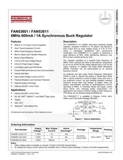
1. 95 1 9 M T 92 90 88 90 86 84 82 80 ut a 85 gt e 2 78 i 0 iam 705 E E ul Bs im 74 72 A 40C AUTO 70 A 25C AUTO eine 85C AUTO 9e 2 7 VIN ae 40C PWM 3 6 VIN 64 esc 25C PWM oun 62 4 85C PWM 70 60 4 0 200 400 600 800 1000 0 200 400 600 800 1000 Load Current mA Load Current mA Figure 4 Efficiency vs Load Current and Figure 5 Efficiency vs Load Current Input Voltage Auto Mode Dotted for Decreasing Load and Temperature Auto Mode Dotted for FPWM 90 90 88 88 86 Bey 84 84 0 82 82 80 gt 80 gt 789 o o 0 76 E 74 W 749 W 72 70 72 689 40C AUTO 70 i 25C AUTO 9 2 7 VIN Add 85C AUTO Eby 3 6 VIN 64 40C PWM 66 4 2 VIN 4 62 25C PWM 64 5 0 VIN 60 EN 85C PWM 0 200 400 600 800 1000 0 200 400 600 800 1000 Load Current mA Load Current mA Figure 6 Efficiency vs Load Current and Figure 7 Efficiency vs Load Current Input Voltage Vout 1 23V Auto Mode Dotted for and Temperature Vout 1 23V Auto Mode Dotted for Decreasing Load FPWM T 3 2 VIN AUTO 2 7VIN AUTO 3 6VIN AUTO 3 6VIN AUTO 4 2VIN AUTO 4 2VIN AUTO2. FAIRCHILD SEMICONDUCTOR FAN53601 FAN53611 6MHz 600mA 1A Synchronous Buck Regulator Features 600mA or 1A Output Current Capability 24pA Typical Quiescent Current 6MHz Fixed Frequency Operation Best in Class Load Transient Response Best in Class Efficiency 2 3V to 5 5V Input Voltage Range 0 8 to 2V Fixed Output Voltage Low Ripple Light Load PFM Mode Forced PWM and External Clock Synchronization Internal Soft Start Input Under Voltage Lockout UVLO Thermal Shutdown and Overload Protection Optional Output Discharge 6 Bump WLCSP 0 4mm Pitch Applications 6 Bump WLCSP 0 4mm Pitch 3G 4G WiFi WiIMAX and WiBro Data Cards Tablets DSC DVC Netbooks Ultra Mobile PCs All trademarks are the property of their respective owners Ordering Information Part Number Voltage FAN53611AUC11X 1 100V LM FAN53601UC182X 1 820V 600mA Notes 1 2 EDU June 2012 Description The FAN53601 11 is a 6MHz step down switching voltage regulator available in 600mA or 1A options that delivers a fixed output from an input voltage supply of 2 3V to 5 5V Using a proprietary architecture with synchronous rectification the FAN53601 11 is capable of delivering a peak efficiency of 92 while maintaining efficiency over 80 at load currents as low as 1mA The regulator operates at a nominal fixed frequency of 6MHz which reduces the value of the external components to as low as 470nH fo
3. Datasheet contains the design specifications for product development Specifications may change in any manner without notice Datasheet contains preliminary data supplementary data will be published at a later date Fairchild First Production Semiconductor reserves the right to make changes at any time without notice to improve design Advance Information Formative In Design Preliminary l Datasheet contains final specifications Fairchild Semiconductor reserves the right to make No Identification Needed Full Production changes at any time without notice to improve the design Natin Production Datasheet contains specifications on a product that is discontinued by Fairchild Semiconductor The datasheet is for reference information only Rev 162 Obsolete www fairchildsemi com 10je nB83J Yong snouoJu2u S y vul009 ZHIN9 LL9 SNV4 LO9ESNVS
4. E PACKAGE TYPICAL HEIGHT IS 586 MICRONS BOTTOM VIEW 39 MICRONS 547 625 MICRONS F FOR DIMENSIONS D E X AND Y SEE PRODUCT DATASHEET G DRAWING FILENAME UCOOG6ACrev4 Figure 1 6 Bump WLCSP 0 4mm Pitch Product Specific Dimensions Product Db E X Y FAN53611AUC11X 1 160 0 030 0 860 0 030 0 230 0 180 FAN53611UC123X 1 160 0 030 0 860 0 030 0 230 0 180 FAN53601UC182X 1 160 0 030 0 860 0 030 0 230 0 180 Package drawings are provided as a service to customers considering Fairchild components Drawings may change in any manner without notice Please note the revision and or date on the drawing and contact a Fairchild Semiconductor representative to verify or obtain the most recent revision Package specifications do not expand the terms of Fairchild s worldwide terms and conditions specifically the warranty therein which covers Fairchild products Always visit Fairchild Semiconductor s online packaging area for the most recent package drawings http www fairchilasemi com packaging 2010 Fairchild Semiconductor Corporation www fairchildsemi com FAN53601 FAN53611 Rev 1 0 0 13 10je nB83J Yong snouoJu2u S y vul009 ZHIN9 LL9 SNV4 LO9ESNVS FAIRCHILD E SEMICONDUEGT HA TRADEMARKS The fallowing includes registered and unregistered trademarks and service marks owned by Fairchild Semiconductor and or its global subsidiaries and is not intended to be an exhaustive list of al
5. Pw oa ne s _ Shutdown suy curen fence os 39 WA Vuno UnderVotage LocoutTiesho Rimos es 22 v Kma Urge oeaan O a 1 Ew Logic Inputs EN and MODE Pins ve ermene 3 KAYA Ww enable aa uvas a Y Wes egewpuHpeessvome mv i Eranio mput Leakage Curent _ Pintovnoreno Om 39 vA Switching and Synchronization t _ Swiching Frequeney ncaov ncmo sa eo 68 ww Regulation lioap O to 1A 1 207 1 233 1 272 V agy Jema OO zT 02899 12722 v Output Voltage ts sons jPomeNmemoEge 99 39 ue Output Driver MOS OnRestionce Ya me fe Opentoop tor Fansen 380 178 2000 ma SS OOO EE ee Te memas ers o Notes 4 Limited by the effect of torr minimum see Operation Description section 5 The Electrical Characteristics table reflects open loop data Refer to the Operation Description and Typical Characteristics Sections for closed loop data 2010 Fairchild Semiconductor Corporation www fairchildsemi com FAN53601 FAN53611 Rev 1 0 0 4 10je nB83J Yong snouoJu2u S y vul009 ZHIN9 LL9 SNV4 LO9ESNVS Typical Performance Characteristics Unless otherwise noted Vin Ven 3 6V Vmode OV AUTO Mode Vour 1 82V and T4 25 C
6. Current mA Figure 32 Frequency vs Load Current to Demonstrate toFFMIN Effect Vin 2 3V and 2 1V Vout 1 82V Auto Mode FPWM Dotted 2010 Fairchild Semiconductor Corporation FAN53601 FAN53611 Rev 1 0 0 The calculation for switching frequency is given by kw min oui SW MAX where tswimax 40NS e I qur ete l w Jour Alon Your where Forr Rpson_n DCR Ron Rpson p DCR www fairchildsemi com Joyeinbay yong snouosyouds y YWO09 ZHIN9 LL9 SNV4 LO9ESNVS Applications Information Selecting the Inductor The output inductor must meet both the reguired inductance and the energy handling capability of the application The inductor value affects average current limit the PWM to PFM transition point output voltage ripple and efficiency The ripple current Al of the regulator is AJ TOUT Vin Your VIN Le fsw 5 The maximum average load current Imax oap IS related to the peak current limit ly iwpi by the ripple current given by Al 6 LIM PK 2 The transition between PFM and PWM operation is determined by the point at which the inductor valley current crosses zero The regulator DC current when the inductor current crosses zero Ipcm is IMAX LOAD Al E 7 DCM 75 7 The FAN53601 11 is optimized for operation with L 470nH but is stable with inductances up to 1uH nominal The inductor should be rated to maintain at lea
7. LL9 SNV4 LO9ESNVS Typical Performance Characteristics Continued Unless otherwise noted Vin Ven 3 6V Vyope OV AUTO Mode Vout 1 82V and Ta 25 C parT ss Phun Da ji i T ajo Cyl ai X Kia LE JB so Tx30300 5 4 ofe 4 2 I Figure 16 Load Transient 10 200 10mA 100ns Edge Der anere 399p 3 MEL ULT edm IRAM a A j r LAMA i i E r8 IL TURN D TR m NNT TTT nN ili rl T e o il X Hija Ie Oh 27 9720000 us aloje T xl 1 Figure 18 Line Transient 3 3 3 9 3 3Vin 10us Edge 36mA Load yor ad 3 al soa 49 ge Aj 4m VIN ANN a LLL LLL mmm eo Gla ua sifon aoe T AL Figure 20 Combined Line Load Transient 3 9 3 3 Vin 10us Edge 36 400mA Load 100ns Edge ao p 38 Unhmw 43 dg MALY 2 erie i gg E le ile eris 3 Hu j ssseee aale af EI T Figure 17 Load Manele dipole 100ns Edge Jet E E a GUT 14 V epe aum VouT IT 2a elo a xxl ass Ha IEEE px afoje Tf ajii E 19 Line Transient 3 3 3 9 3 3Vin 10us Edge 600mA Load Je arm Bre or AINA META IA IAA n ajo c3 s 3 H Dusi E LI 4 480000 ps dole l f I Figure 21 Combined Line Load Transient 3 3 3 9Vin 10us Edge 400 36mA Load 100ns Edge 3 9 3 3 Vin 10us Edge Be 212 ADAS EO EI ajs cx ia sos keel aale Tomy sii Figure 22 Startup 500 Load 2010 Fairchild Semi
8. part and starts the soft start cycle During soft start the internal reference is ramped using an exponential RC shape to prevent overshoot of the output voltage Current limiting minimizes inrush during soft start The current limit fault response protects the IC in the event of an over current condition present during soft start As a result the IC may fail to start if heavy load is applied during startup and or if excessive Cour is used 2010 Fairchild Semiconductor Corporation FAN53601 FAN53611 Rev 1 0 0 The current required to charge Cou during soft start commonly referred to as displacement current is given as dV Ipisp Cour pn 1 where refers to the soft start slew rate To prevent shut down during soft start the following condition must be met IpisP ILoAD lt IMAX DC 2 where IMAX DC is the maximum load current the IC is guaranteed to support Startup into Large Cour Multiple soft start cycles are required for no load startup if Cou is greater than 15uF Large Cou requires light initial load to ensure the FAN53601 11 starts appropriately The IC shuts down for 1 3ms when lIpisp exceeds lumt for more than 200us of current limit The IC then begins a new soft start cycle Since Cour retains its charge when the IC is off the IC reaches regulation after multiple soft start attempts MODE Pin Logic 1 on this pin forces the IC to stay in PWM Mode A logic O allows the IC to automatic
9. 0 20 0 1 1 10 100 1000 0 1 1 10 100 1000 Frequency KHz Frequency KHz Figure 30 PSRR 500 and 3O Load Figure 31 PSRR 500 and 30 Load Vout 1 23V 2010 Fairchild Semiconductor Corporation www fairchildsemi com FAN53601 FAN53611 Rev 1 0 0 8 10je nB83J Yong snouoJu2u S y vul009 ZHIN9 LL9 SNV4 LO9ESNVS Operation Description The FAN53601 11 is a 6MHZ step down switching voltage regulator available in 600mA or 1A options that delivers a fixed output from an input voltage supply of 2 3V to 5 5V Using a proprietary architecture with synchronous rectification the FAN53601 11 is capable of delivering a peak efficiency of 92 while maintaining efficiency over 80 at load currents as low as 1mA The regulator operates at a nominal fixed frequency of 6MHz which reduces the value of the external components to as low as 470nH for the output inductor and 4 7uF for the output capacitor In addition the PWM modulator can be synchronized to an external frequency source Control Scheme The FAN53601 11 uses a proprietary non linear fixed frequency PWM modulator to deliver a fast load transient response while maintaining a constant switching frequency over a wide range of operating conditions The regulator performance is independent of the output capacitor ESR allowing for the use of ceramic outp
10. 5 0VIN AUTO 2 5 0VIN AUTO 2 7VIN PWM a 2 7VIN PWM S 3 6VIN PWM as e Me 3 6VIN PWM c 4 2VIN PWM c OS dae aed 4 VIN PWM 9 5 0VIN PWM S IS 5 0VIN PWM S S TRI j 3 i D Loz Q c c me 5 5 Q Q 5 5 O O 1 2 400 600 800 1000 0 200 400 600 800 1000 Load Current mA Load Current mA Figure 8 AVout Yo vs Load Current and Input Voltage Figure 9 AVout Yo vs Load Current and Input Voltage Normalized to 3 6Vin 500mA Load FPWM Dotted for Vout 1 23V Normalized to 3 6Vin 500mA Load FPWM Auto Mode Dotted for Auto Mode 2010 Fairchild Semiconductor Corporation www fairchildsemi com FAN53601 FAN53611 Rev 1 0 0 5 10je nB83J Yong snouoJu2u S y vul009 ZHIN9 LL9 SNV4 LO9ESNVS Typical Performance Characteristics Continued Unless otherwise noted Vin Ven 3 6V Vmode OV AUTO Mode Vour 1 82V and Ta 25 C 350 350 300 300 PTE rr 250 250 E E t r 200 200 gt gt o o 150 150 100 100 PWM PWM PFM PFM 50 50 2 5 3 0 3 5 4 0 4 5 5 0 5 5 2 5 3 0 3 5 4 0 4 5 5 0 5 5 Input Voltage V Input Voltage V Figure 10 PFM PWM Boundary vs Input Voltage Figure 11
11. ICE TO ANY PRODUCTS HEREIN TO IMPROVE RELIABILITY FUNCTION OR DESIGN FAIRCHILD DOES NOT ASSUME ANY LIABILITY ARISING OUT OF THE APPLICATION OR USE OF ANY PRODUCT OR CIRCUIT DESCRIBED HEREIN NEITHER DOES IT CONVEY ANY LICENSE UNDER ITS PATENT RIGHTS NOR THE RIGHTS OF OTHERS THESE SPECIFICATIONS DO NOT EXPAND THE TERMS OF FAIRCHILD S WORLDWIDE TERMS AND CONDITIONS SPECIFICALLY THE WARRANTY THEREIN WHICH COVERS THESE PRODUCTS LIFE SUPPORT POLICY FAIRCHILD S PRODUCTS ARE NOT AUTHORIZED FOR USE As CRITICAL COMPONENTS IN LIFE SUPPORT DEVICES OR SYSTEMS WITHOUT THE EXPRESS WRITTEN APPROVAL OF FAIRCHILD SEMICONDUCTOR CORPORATION As used herein 1 Life support devices or systems are devices or systems which a are 2 A critical component in any component of a life support device or intended for surgical implant into the body or b support or sustain system whose failure to perform can be reasonably expected to life and c whose failure to perform when properly used in cause the failure of the life support device or system or to affect its accordance with instructions for use provided in the labeling can be safety or effectiveness reasonably expected to result in a significant injury of the user ANTI COUNTERFEITING POLICY Fairchild Semiconductor Corporation s Anti Counterteiting Policy Fairchild s Anti Counterteiting Policy is also stated on our extemal website www fairchildsemi com under Sales Support Counterfeiting of semiconducto
12. PFM PWM Boundary vs Input Voltage Vout 1 23V 35 15 40C EN VIN 40C 25C EN VIN 25C 85C EN VIN 85C 40C EN 1 8V zA 12 30 T 25C EN 1 8V Js T 85C EN 1 8V Jobe SB FJ LL thi tp Gg B BL pd dd cto ble ki E e 5 0 db4 t 7T 7 cri 9 z z S om 2 5 e 20 3 15 0 2 5 3 0 3 5 4 0 4 5 5 0 5 5 2 5 3 0 3 5 4 0 4 5 5 0 5 5 Input Voltage V Input Voltage V Figure 12 Guiescent Current vs Input Voltage and Figure 13 Guiescent Current vs Input Voltage and Temperature Auto Mode EN Vin Solid Dotted for Temperature Mode EN Vin FPWM EN 1 8V 40 C 25 C 85 C 25 7 500 2 7VIN AUTO 3 6VIN AUTO 5 0VIN AUTO d 20 amp 2 7VIN PWM N 6 000 E fsd z Y 3 6VIN PWM x 2 LA pet vA 5 0VIN PWM gt 15 WX S 4 500 2 W A S X A 10 4 3 000 amp S TAM 2 7VIN AUTO 5 TS 2 3 6VIN AUTO gt Moores rr id gt 5 0VIN AUTO 5 O 1 500 ee 2 7VIN PWM 3 6VIN PWM o 5 0VIN PWM 0 200 400 600 800 1000 0 200 400 600 800 1000 Load Current mA Load Current mA Figure 14 Output Ripple vs Load Current and Figure 15 Frequency vs Load Current and Input Voltage FPWM Dotted for Auto Mode Input Voltage Auto Mode Dotted for FPWM 2010 Fairchild Semiconductor Corporation www fairchildsemi com FAN53601 FAN53611 Rev 1 0 0 6 Joyeinbay yong snouoJu2u S y vul009 ZHIN9
13. Up Pin Definitions Pint Name aterm MODE Logic 1 on this pin forces the IC to stay in PWM Mode A logic 0 allows the IC to A1 MODE X automatically switch to PFM during light loads The regulator also synchronizes its switching frequency to four times the frequency provided on this pin Do not leave this pin floating Switching Node Connect to output inductor Feedback Vour Connect to output voltage Ground Power and IC ground All signals are referenced to this pin B2 EN Enable The device is in Shutdown Mode when voltage to this pin is 0 4V and enabled when 1 2V Do not leave this pin floating Input Voltage Connect to input power source 2010 Fairchild Semiconductor Corporation www fairchildsemi com FAN53601 FAN53611 Rev 1 0 0 2 Joyeinbay yong snouoJu2u S vj vul009 ZHIN9 LL9 SNV4 LO9ESNVS Absolute Maximum Ratings Stresses exceeding the absolute maximum ratings may damage the device The device may not function or be operable above the recommended operating conditions and stressing the parts to these levels is not recommended In addition extended exposure to stresses above the recommended operating conditions may affect device reliability The absolute maximum ratings are stress ratings only Symol Parameter Mi Max Units op Electrostatic Discharge Human Body Model per JESD22 A114 m Protection Level Charged Device Model per JESD22 C101 Junction Temperature Lead Solderin
14. ally switch to PFM during light loads If the MODE pin is toggled with a frequency between 1 3MHz and 1 7MHz the converter synchronizes its switching frequency to four times the frequency on the MODE pin The MODE pin is internally buffered with a Schmitt trigger which allows the MODE pin to be driven with slow rise and fall times An asymmetric duty cycle for frequency synchronization is also permitted as long as the minimum time below ViL MAX or above ViH MAX is 100ns Current Limit Fault Shutdown and Restart A heavy load or short circuit on the output causes the current in the inductor to increase until a maximum current threshold is reached in the high side switch Upon reaching this point the high side switch turns off preventing high currents from causing damage The regulator continues to limit the current cycle by cycle After 16 cycles of current limit the regulator triggers an over current fault causing the regulator to shut down for about 1 3ms before attempting a restart If the fault is caused by short circuit the soft start circuit attempts to restart and produces an over current fault after about 200us which results in a duty cycle of less than 15 limiting power dissipation The closed loop peak current limit is not the same as the open loop tested current limit lior in the Electrical Characteristics table This is primarily due to the effect of propagation delays of the IC current limit comparator www fai
15. conductor Corporation FAN53601 FAN53611 Rev 1 0 0 nfl 2s 7420000 LE aloje Tyr vi T Figure 23 Startup 30 Load zl e e Gis OE www fairchildsemi com Joyeinbay yong snouosyouds y vul009 ZHIN9 LL9 SNV4 LO9ESNVS Typical Performance Characteristics Continued Unless otherwise noted Vin Ven 3 6V Vwope OV Mode Vout 1 82V and Ta 25 E el yapm YIr 4 p io 38 A ag we sg fe m ua EIS T EN p I ele sis H ay NU ni ol as i E r umm 4 ele Cae XE HE T aja JE XX m afoje T PLI Figure 24 SS 10k Load No gt Output Discharge Figure 25 Shutdown No Load i Output Discharge Enabled F x jgpss Mb ggpew 23g jg jgpew ap agp ua IL L I l i fta t 4 e o css 3s H 1 00 ms Vers OO ms oir ej c jocis x rcm ajas afoje r e5m Figure 26 Over Current Load Siha Sasia Past Current Figure 27 250mQ Fault Rapid F Fault Hiccup FAN53601 Limit FAN53601 On 2 E T 3 ony x 4 n Vout m m z Aa jha ea Dr lia neve AE cen 5994 aepo woes sieo Joly r wtm ei Figure 28 Over Current Load easing Past Current Figure 29 250mO Fault Rapid F Fault Hiccup FAN53611 Limit FAN53611 70 70 36mA Load 24mA Load 600mA Load 500mA Load 60 r H oO 50 2 fe fe P w 5 30 2
16. g Temperature 10 Seconds 920 C Note 3 Lesser of 7V or Vint0 3V Recommended Operating Conditions The Recommended Operating Conditions table defines the conditions for actual device operation Recommended operating conditions are specified to ensure optimal performance to the datasheet specifications Fairchild does not recommend exceeding them or designing to Absolute Maximum Ratings symb Panmeer Mi Typ Max Units we mewvwaeRame 23 88 V Output Current for FAN53601 Output Current for FAN5361 1 mad o 49 mM Thermal Properties Junction to ambient thermal resistance is a function of application and board layout This data is measured with four layer 1s2p boards in accordance to JEDEC standard JESD51 Special attention must be paid to not exceed junction temperature T ymax at a given ambient temperate Ta Symbol Parameter Typical Unit Junction to Ambient Thermal Resistance 2010 Fairchild Semiconductor Corporation www fairchildsemi com FAN53601 FAN53611 Rev 1 0 0 3 10je nB83J yong snouoJu2u S vj vuI009 ZHIN9 LL9 SNV4 LO9ESNVS Electrical Characteristics Minimum and maximum values are at Vin Ven 2 3V to 5 5V Vmode OV AUTO Mode Ta 40 C to 85 C circuit of Figure 1 unless otherwise noted Typical values are at TA 25 C Vin Ven 3 6V Symbol Parameter conditons vin Ty Max Unis Power Supplies
17. l such trademarks 2Coal F PFS PowerTrench The Power Franchise AccuPower FRFET Powerxs the AX CAp Global Power Resource Programmable Active Droop P We F BitSicr GreenBridge QFET TinvBoost Build it Now Green FPS QS aa CorePLUS Green FPS e Series Quiet Senes Mui eae CorePOWER Gmax RapidConfigure Tiny ogic CROSSVOLT GTO eu TINYOPTO CTL InteilliAx Saving our world 1mVV AW KW at a time TinyPower Current Transfer Logic ISOPLANAR SignalWise TinyPWIWr I8 1 i DEUXPEED Making Small Speakers Sound Louder SmartMax TinyWire Dual Coal and Better n i SMART START Transic EcoSPARK MegaBuck Solutions for Y our Success TriFault Detect EfficientMax MICROCOUPLER D l SPM TRUECURRENT ESBc MicroFET W F MicroPak Babes uSerDes c up MicroPak2 eed M WA Fairchild Miller Drive Ted i Des Fairchild Semiconductor MofienMa y SuperSOT 6 UHC FACT Quiet Series supersOT 8 Ultra FRFET mW Saver FACT OptoHiT SupreMOS UniFET SyncFET Th FAST OPTOLOGIC FS aT VOAN FETBench dane EM os VoltagePlus FlashWriter xs FPs 7 Trademarks of System General Corporation used under license by Fairchild Semiconductor DISCLAIMER 2010 Fairchild Semiconductor Corporation FAN53601 FAN53611 Rev 1 0 0 14 FAIRCHILD SEMICONDUCTOR RESERVES THE RIGHT TO MAKE CHANGES WITHOUT FURTHER NOT
18. ntalum should be placed between Cin and the power source lead to reduce the ringing that can occur between the inductance of the power source leads and Cw The effective capacitance value decreases as Vin increases due to DC bias effects Table 1 Effects of Changes in Inductor Value from 470nH Recommended Value on Regulator Performance Iesse increase Decrease Decrease Decrease Increase Degraded Improved Table 2 Recommended Passive Components and their Variation Due to DC Bias Component Description Vendor Mim Typ max Murata LQM21PNR47MCO Murata LQM21PNR54MGO Hitachi Metals HLSI 201210R47 470nH 2012 90mQ 1 1A 300nH 470nH 520nH C 2 2uF 6 3V Murata or Equivalent GRM155R60J225ME15 10uF 2 ONE X5R 0402 GRM188R60J225KE19D iss r Murata or Equivalent GRM155R60G475M 2010 Fairchild Semiconductor Corporation FAN53601 FAN53611 Rev 1 0 0 www fairchildsemi com 10je nB83J Yong snouoJu2u S vj vuI009 ZHIN9 LL9 SNV4 LO9ESNVS PCB Layout Guidelines There are only three external components the inductor and the input and output capacitors For any buck switcher IC including the FAN53601 11 it is important to place a low ESR input capacitor very close to the IC as shown in Figure 33 The input capacitor ensures good input decoupling which helps reduce noise appearing at the output terminals and ensures that the control sections of the IC do not behave er
19. r parts is a growing problem in the industry All manufacturers of semiconductor products are experiencing counterfeiting of their parts Customers who inadvertently purchase counterfeit parts experience many problems such as loss of brand reputation substandard performance failed applications and increased cost of production and manufacturing delays Fairchild is taking strong measures to protect ourselves and our customers from the proliferation of counterfeit parts Fairchild strongly encourages customers to purchase Fairchild parts either directly from Fairchild or from Authorized Fairchild Distributors who are listed by country on our web page cited above Products customers buy either from Fairchild directly or from Authorized Fairchild Distributors are genuine parts have full traceability meet Fairchild s quality standards for handling and storage and provide access to Fairchild s full range of up to date technical and product information Fairchild and our Authorized Distributors will stand behind all warranties and will appropriately address any warranty issues that may arise Fairchild will not provide any warranty coverage or other assistance for parts bought from Unauthorized Sources Fairchild is committed to combat this global problem and encourage our customers to do their part in stopping this practice by buying direct or from authorized distributors PRODUCT STATUS DEFINITIONS Definition of Terms Datasheet Identification Product Status
20. r the output inductor and 4 7uF for the output capacitor In addition the Pulse Width Modulation PWM modulator can be synchronized to an external frequency source At moderate and light loads Pulse Frequency Modulation PFM is used to operate the device in Power Save Mode with a typical quiescent current of 24uA Even with such a low quiescent current the part exhibits excellent transient response during large load swings At higher loads the system automatically switches to fixed frequency control operating at 6MHz In Shutdown Mode the supply current drops below 1pA reducing power consumption For applications that require minimum ripple or fixed frequency PFM Mode can be disabled using the MODE pin The FAN53601 11 is available in 6 bump 0 4mm pitch Wafer Level Chip Scale Package WLCSP Figure 1 Typical Application Max Output Active Package Temperature Current L g Range WLCSP 6 Tape and 0 4mm Pitch 40 to 99 C Bea Other voltage options available on request Contact a Fairchild representative 2010 Fairchild Semiconductor Corporation FAN53601 FAN53611 e Rev 1 0 0 All voltage and output current options are available with or without active discharge Contact a Fairchild representative www fairchildsemi com Joyeinbay Yong SnouoJyJuAs y vul009 ZHIN9 LL9 ESNV4 LO9ESNVS Pin Configurations MODE VIN VIN MODE SW EN FB GND Figure 2 Bumps Facing Down Figure 3 Bumps Facing
21. ratically due to excessive noise This reduces switching cycle jitter and ensures good overall performance It is important to place the common GND of Cin and Cour as close as possible to the C2 terminal There is some flexibility in moving the inductor further away from the IC in that case Vout should be considered at the Cour terminal Figure 33 PCB Layout Guidance 2010 Fairchild Semiconductor Corporation FAN53601 FAN53611 Rev 1 0 0 www fairchildsemi com 10je nB83J Yong snouoJu2u S vj vul009 ZHIN9 LL9 SNV4 LO9ESNVS Physical Dimensions F gt 0 03 C 2X E A B 7 040 BALLAT i 90 20 INDEK AREA BI A Cu Pad D YA 0 40 Solder Mask 0 03 C Opening 2X TOP VIEW RECOMMENDED LAND PATTERN NSMD PAD TYPE 0 06 C i 0 378 0 018 0 625 Yvi gt d CH _ SEATING PLANE D SIDE VIEWS 0 260 0 010 NOTES 6X mU ry E TE A NO JEDEC REGISTRATION APPLIES toy r B DIMENSIONS ARE IN MILLIMETERS c B Y 0 018 C DIMENSIONS AND TOLERANCES PER 0 40 5 z ASMEY14 5M 1994 ES i pes D DATUM C THE SEATING PLANE IS DEFINED 1 2 pus BY THE SPHERICAL CROWNS OF THE BALLS a SPOS
22. rchildsemi com 10je nB83J Yong snouoJu2u S y vul009 ZHIN9 LL9 SNV4 LO9ESNVS Under Voltage Lockout UVLO When EN is HIGH the under voltage lockout keeps the part from operating until the input supply voltage rises high enough to properly operate This ensures no misbehavior of the regulator during startup or shutdown Thermal Shutdown TSD When the die temperature increases due to a high load condition and or a high ambient temperature the output switching is disabled until the die temperature falls sufficiently The junction temperature at which the thermal shutdown activates is nominally 150 C with a 15 C hysteresis Minimum Off Time Effect on Switching Frequency torF uiN IS 40ns This imposes constraints on the maximum Your that the FAN53601 11 can provide or the maximum IN output voltage it can provide at low Vin while maintaining a fixed switching frequency in PWM Mode When Vin is LOW fixed switching is maintained as long as V OUT c AEN IN orrn 9 fsw 20 7 The switching frequency drops when the regulator cannot provide sufficient duty cycle at 6MHz to maintain regulation This occurs when Vout is 1 82V and Vin is below 2 7V at high load currents see Figure 32 7 500 6 000 2 7VIN AUTO 2 3VIN AUTO 2 7VIN PWM 2 3VIN PWM 3 000 Switching Frequency KHz 1 500 0 200 400 600 800 1000 Load
23. st 80 of its value at ILimek Efficiency is affected by the inductor DCR and inductance value Decreasing the inductor value for a given physical size typically decreases the DCR but because Al increases the RMS current increases as do the core and skin effect losses Al 2 Ins 4 lout oc TE 8 The increased RMS current produces higher losses through the Rps on of the IC MOSFETs as well as the inductor DCR Increasing the inductor value produces lower RMS currents but degrades transient response For a given physical inductor size increased inductance usually results in an inductor with lower saturation current and higher DCR Table 1 shows the effects of inductance higher or lower than the recommended 14H on regulator performance Output Capacitor Table 2 suggests 0402 capacitors 0603 capacitors may further improve performance in that the effective capacitance is higher This improves transient response and output ripple Increasing Court has no effect on loop stability and can therefore be increased to reduce output voltage ripple or to improve transient response Output voltage ripple AVour is fe ME ER 1 Bor Al ER OUT L n e CU ENTIS 9 SW OUT Input Capacitor The 2 2uF ceramic input capacitor should be placed as close as possible between the VIN pin and GND to minimize the parasitic inductance If a long wire is used to bring power to the IC additional bulk capacitance electrolytic or ta
24. ut capacitors Although this type of operation normally results in a switching frequency that varies with input voltage and load current an internal frequency loop holds the switching frequency constant over a large range of input voltages and load currents For very light loads the FAN53601 11 operates in discontinuous current DCM single pulse PFM Mode which produces low output ripple compared with other PFM architectures Transition between PWM and PFM is seamless allowing for a smooth transition between DCM and CCM Combined with exceptional transient response characteristics the very low quiescent current of the controller maintains high efficiency even at very light loads while preserving fast transient response for applications requiring tight output regulation Enable and Soft Start When EN is LOW all circuits are off and the IC draws 50nA of current When EN is HIGH and Vin is above its UVLO threshold the regulator begins a soft start cycle The output ramp during soft start is a fixed slew rate of 50mV us from 0 to 1 Vout then 12 5mV us until the output reaches its setpoint Regardless of the state of the MODE pin PFM Mode is enabled to prevent current from being discharged from Court if soft start begins when Cour is charged In addition all voltage options can be ordered with a feature that actively discharges FB to ground through a 230 path when EN is LOW Raising EN above its threshold voltage activates the
Download Pdf Manuals

Related Search
FAIRCHILD FAN53601 Manual