Allegro A3241 A3242 Manual
Contents
1. Continued on the next page gam Allegro MicroSystems Inc 4 Toor 115 Northeast Cutoff Box 15036 a mm mm A3241 DS Rev 2 LUE a Worcester Massachusetts 01615 0036 508 853 5000 ann NP MicroSystems Inc www allegromicro com A3241 and A3242 Chopper Stabilized Unipolar Hall Effect Switches Operate Point versus Ambient Temperature Operate Point versus Supply Voltage A3241 A3241 Release Point versus Ambient Temperature Release Point versus Supply Voltage A3241 A3241 Hysteresis versus Supply Voltage Hysteresis versus Ambient Temperature A3241 A3241 ee Ta C n eT 40 25 150 Allegro MicroSystems Inc 5 115 Northeast Cutoff Box 15036 Worcester Massachusetts 01615 0036 508 853 5000 www allegromicro com A3241 DS Rev 2 A3241 and A3242 Chopper Stabilized Unipolar Hall Effect Switches Operate Point versus Ambient Temperature A3242 Release Point versus Ambient Temperature A3242 Hysteresis versus Ambient Temperature A3242 Vcc V 24 25 3 62. A3241 DS Rev 2 150 Operate Point versus Supply Voltage A3242 Release Point versus Supply Voltage A3242 Hysteresis versus Supply Voltage A3242 Allegro MicroSystems Inc 6 115 Northeast Cutoff Box 15036 Worcester Massachusetts 01615 0036 508 853 5000 www allegromicro com A3241 and A3242 Chopper Stabilized Unipolar Hall Effect Switches THERMAL CHARACTERISTICS may require derating at maximum conditions see application information Characteristic Symbol Test Conditions Value Units Package LH 3 1 layer PCB with copper limited to 110 eC AW solder pads Package LH 3 2 layer PCB with 0 926 in2 on each Package Thermal Resistance Roya side ea d by Md Vias C W Package UA 1 layer PCB with copper limited to 165 eC W solder pads Power Derating Curve 1 layer PCB Package LH R oya 110 C W 1 layer PCB Package UA Rasa 165 C W 2 layer PCB Package LH R aa 228 C W 13 Maximum Allowable Vcc V r NOB O10 N00 O NO Vcc min 20 40 60 80 100 120 140 160 180 Temperature C Power Dissipation versus Ambient Temperature 20 40 60 80 100 120 140 160 180 Temperature C Allegro MicroSystems Inc T 115 Northeast Cutoff Box 15036 Worcester M
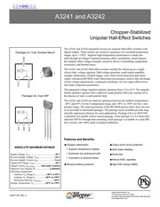
3. 0 0 A324 OO A3241 and A3242 Package LH 3 pin Surface Mount Q Z Q Ee D O gt Package UA 3 pin SIP Jj 2 3 ABSOLUTE MAXIMUM RATINGS Supply Voltage Vcc Reverse Supply Voltage Vecc Reverse Supply Current Ipcc Output Off Voltage Vou Output Current IouTsINK Magnetic Flux Density B Operating Temperature Ambient Ta Range E Ambient T4 Range L Maximum Junction TiMax Storage Temperature Ts Internally Limited Unlimited 40 C to 85 C 40 C to 150 C 65 C to 170 C A3241 DS Rev 2 Chopper Stabilized Unipolar Hall Effect Switches The A3241 and A3242 integrated circuits are unipolar Hall effect switches with digital outputs These sensors are suited for operation over extended temperature ranges up to 150 C Superior high temperature performance is made pos sible through an Allegro patented dynamic offset cancellation which reduces the residual offset voltage normally caused by device overmolding temperature excursions and thermal stress The A3241 and A3242 Hall effect switches include the following on a single silicon chip voltage regulator Hall voltage generator small signal amplifier chopper stabilization Schmitt trigger and a short circuit protected open drain output Advanced BiCMOS wafer fabrication processing is used to take advantage of low voltage requirements component matching very low input offset errors and small component geometries The integrat
4. 03 1 Soldering Methods for Allegro s Products SMT and Through Powering on the device in the hysteresis region less than Bop Hole AN26009 and higher than Brp allows an indeterminate output state The correct state is attained after the first excursion beyond Bop or All are provided in Allegro Electronic Data Book AMS 702 and Bpp the Allegro Web site www allegromicro com A B Vs Vcc Ex da RLOAD O I a O 2 2 Sensor Output ps g A324x VOUT 5 O VOUT SAT Figure 1 Switching Behavior of Unipolar Switches In Panel A on the horizontal axis the B4 direction indicates increasing south polarity magnetic field strength and the B direction indicates decreasing south polarity field strength including the case of increasing north polarity This behavior can be exhibited when using a circuit such as that shown in panel B Allegro MicroSystems Inc 8 115 Northeast Cutoff Box 15036 Worcester Massachusetts 01615 0036 508 853 5000 www allegromicro com A3241 DS Rev 2 A3241 and A3242 Chopper Stabilized Unipolar Hall Effect Switches Chopper Stabilization Technique When using Hall effect technology a limiting factor for switchpoint accuracy is the small signal voltage developed across the Hall element This voltage is disproportionally small relative to the offset that can be produced at the output of the Hall sensor This makes it difficult to process the signal while maintaining an
5. 40 to 150 Contact Allegro for additional packing options Functional Block Diagram son EE Sample and Hold Description Package LH Package UA i 1 Allegro MicroSystems Inc 2 115 Northeast Cutoff Box 15036 Worcester Massachusetts 01615 0036 508 853 5000 www allegromicro com A3241 DS Rev 2 A3241 and A3242 Chopper Stabilized Unipolar Hall Effect Switches OPERATING CHARACTERISTICS valid over full operating voltage and ambient temperature ranges unless otherwise noted Characteristic Symbol Test Conditions in Typ Max Unite Supiy vones J Wu oaa 185 o 7 V Output Leakage Curent touro VozMVBsBe 9 OupstOnVotag Vom llour 20MA B gt Bop wm Powerontme wo Mu Vumw of Shopping Frequency SSS 89 _ Ouputrise Time f Ronca fefe Owmwra me Rn 8200 65 T A Remo e a E EEEE mor Beee 318 38 m Reverse Batery Curent Meo Moose o o Cm Magnetic Characteristics so Ts es e Operate Point Bop terete M M0 125 190 e 1 Maximum voltage must be adjusted for power dissipation and junction temperature see Power Derating section 2 Cs oscilloscope probe capacitance 3 Maximum current limit is equal to the maximum lcc max 3 mA Magnetic flux density B is indicated as a negative value for north polarity magnetic fields and as a positive value for south polarity magnet
6. accurate reliable output over the specified oper ating temperature and voltage ranges Chopper stabilization is a unique approach used to minimize Hall offset on the chip The patented Allegro technique namely Dynamic Quadrature Offset Cancellation removes key sources of the output drift induced by thermal and mechanical stresses This offset reduction technique is based on a signal modulation demodulation process The undesired offset signal is separated from the magnetic field induced signal in the frequency domain through modulation The subsequent demodulation acts as a modulation process for the offset causing the magnetic field induced signal to recover its original spectrum at baseband while the dc offset becomes a high frequency signal The mag netic field induced signal then can pass through a low pass filter while the modulated dc offset is suppressed This configuration is illustrated in figure 2 Regulator Hall Element 4r Clock Logic The chopper stabilization technique uses a 200 kHz high fre quency clock For demodulation process a sample and hold technique is used where the sampling is performed at twice the chopper frequency 400 kHz This high frequency operation allows a greater sampling rate which results in higher accuracy and faster signal processing capability This approach desensi tizes the chip to the effects of thermal and mechanical stresses and produces devices that have extremely stable qu
7. assachusetts 01615 0036 508 853 5000 www allegromicro com A3241 DS Rev 2 a 1E m E MicroSystems Inc A3241 and A3242 Chopper Stabilized Unipolar Hall Effect Switches Functional Description Operation Applications The output of these devices switches low turns on when a It is strongly recommended that an external bypass capacitor be magnetic field south polarity perpendicular to the Hall sen connected in close proximity to the Hall sensor between the sor exceeds the operate point threshold Bop After turn on the supply and ground of the device to reduce both external noise output voltage is Voyrgary The output transistor is capable of and noise generated by the chopper stabilization technique As is sinking current up to the short circuit current limit Ig which shown in Panel B of figure 1 a 0 1uF capacitor is typical is a minimum of 30 mA When the magnetic field is reduced Extensive applications information on magnets and Hall effect below the release point Bgp the device output goes high turns sensors is available in off The dierenee in the magnetic operate and release Points is Hall Effect IC Applications Guide AN27701 the hysteresis Buys of the device This built in hysteresis allows clean switching of the output even in the presence of external Hall Effect Devices Gluing Potting Encapsulating Lead mechanical vibration and electrical noise Welding and Lead Forming AN277
8. cally Raza 7228 C W Timas 165 C Voca 24 V and lec max 5 MA Calculate the maximum allowable power level Pp First invert equation 3 AL us Tica lA 165 C 150 C 15 C This provides the allowable increase to T resulting from internal power dissipation Then invert equation 2 Finally invert equation 1 with respect to voltage Vcc es Pogmax lcc max 605 8mW 5 mA 13 2 V The result indicates that at T4 the application and device can dissipate adequate amounts of heat at voltages SVcc esp Compare Vcctest to V CC max If Vcctest lt V cc max gt then reli able operation between Vcc est and Vec maxy requires enhanced Roya If Vocrest 2 Voc max then operation between Veces and Voccmax 1 reliable under these conditions Allegro MicroSystems Inc 1 O 115 Northeast Cutoff Box 15036 A3241 DS Rev 2 Worcester Massachusetts 01615 0036 508 853 5000 www allegromicro com A3241 and A3242 Chopper Stabilized Unipolar Hall Effect Switches Package LH 3 Pin SOT 23W 3 10 122 290 114 a 149 059 2 070 028 gt j SJ se ss al 094 0 25 010 MIN z 11 0 d BSC I E 037 025 010 BSC Sealing Piana Dimensions in millimeters Gauge Plane U S Customary dimensions in in brackets for reference only A Hall element AX Active Area Depth 0 28 L011 A Fits SC 59A Solder Pad Layout adjust to process
9. ed voltage regulator permits operation from 3 6 to 24 V The unipolar family members operate with a sufficient south polarity field only turning off in the absence of such a south polarity field The A3241 and A3242 are rated for operation between the ambient temperatures 40 C and 85 C for the E temperature range and 40 C to 150 C for the L tem perature range The small geometries of the BiCMOS process allow these devices to be provided in ultrasmall packages The package styles available provide mag netically optimized solutions for most applications Package LH is an SOT23W a miniature low profile surface mount package while package UA is a three lead ultramini SIP for through hole mounting Each package 1s available in a lead Pb free version with 100 matte tin plated leadframes Features and Benefits m Chopper stabilization e Superior temperature stability e Extremely low switchpoint drift Insensitive to physical stress Bi Reverse battery protection E Output short circuit protection B Solid state reliability B Small size m Robust EMC capability m High ESD ratings HBM Allegro MicroSystems Inc 115 Northeast Cutoff Box 15036 Worcester Massachusetts 01615 0036 508 853 5000 www allegromicro com A3241 and A3242 Chopper Stabilized Unipolar Hall Effect Switches Product Selection Guide teil lt 7 in reel 3000 pieces reel 40 135 40 to 150 40 to 85 110 200
10. ic fields This so called algebraic convention supports arithmetic comparison of north and south polarity values where the relative strength of the field is indicated by the absolute value of B and the sign indicates the polarity of the field for example a 100 G field and a 100 G field have equivalent strength but opposite polarity DEVICE QUALIFICATION PROGRAM Contact Allegro for information EMC Electromagnetic Compatibility REQUIREMENTS Contact Allegro for information Allegro MicroSystems Inc 3 115 Northeast Cutoff Box 15036 Worcester Massachusetts 01615 0036 508 853 5000 www allegromicro com A3241 DS Rev 2 A3241 and A3242 Chopper Stabilized Unipolar Hall Effect Switches Characteristic Data Supply Current On versus Ambient Temperature Supply Current On versus Supply Voltage 5 0 4 0 T 3 0 Vcc V A a 24 E 2 0 ee 30 8 i D 1 0 0 0 50 0 50 100 150 Supply Current Off versus Ambient Temperature Supply Current Off versus Supply Voltage Iccorr mA Iccorr mA Output Voltage On versus Ambient Temperature Output Voltage On versus Supply Voltage Vour sar mV NNO
11. ied power or improving the heat dissipation properties of the application This section presents a procedure for correlating factors affecting operating Tj Thermal data is also available on the Allegro MicroSystems Web site The Package Thermal Resistance Roj 4 is a figure of merit sum marizing the ability of the application and the device to dissipate heat from the junction die through all paths to the ambient air Its primary component is the Effective Thermal Conductivity K of the printed circuit board including adjacent devices and traces Radiation from the die through the device case Rojc is relatively small component of Rgj4 Ambient air temperature T4 and air motion are significant external factors damped by overmolding The effect of varying power levels Power Dissipation Pp can be estimated The following formulas represent the fundamental relationships used to estimate T at Pp AT Pp X Rosa 2 For example given common conditions such as T 25 C Voc 12 V lec 1 5 mA and Roya 165 C W then Pp Vec X Icc 12V x 1 5 mA 18 mW AT Pp X Rosa 18 mW x 165 C W 3 C Ty T AT 25 C 3 C 28 C A worst case estimate Pp max represents the maximum allow able power level Vcc max gt Lcc max Without exceeding Timax at a selected Roy and Ty Example Reliability for Vcc at T4 150 C package LH using a low K PCB Observe the worst case ratings for the device specifi
12. iescent Hall output voltages and precise recoverability after temperature cycling This technique is made possible through the use of a BiCMOS process which allows the use of low offset low noise amplifiers in combination with high density logic integration and sample and hold circuits The repeatability of magnetic field induced switching is affected slightly by a chopper technique However the Allegro high frequency chopping approach minimizes the affect of jitter and makes it imperceptible in most applications Applications that are more likely to be sensitive to such degradation are those requiring precise sensing of alternating magnetic fields for example speed sensing of ring magnet targets For such applica tions Allegro recommends its digital sensor families with lower sensitivity to jitter For more information on those devices contact your Allegro sales representative Sample and Low Pass Filter Figure 2 Chopper Stabilization Circuit Dynamic Quadrature Offset Cancellation Allegro MicroSystems Inc 9 115 Northeast Cutoff Box 15036 A3241 DS Rev 2 Worcester Massachusetts 01615 0036 508 853 5000 www allegromicro com A3241 and A3242 Chopper Stabilized Unipolar Hall Effect Switches Power Derating The device must be operated below the maximum junction temperature of the device Timax Under certain combinations of peak conditions reliable operation may require derating sup pl
13. legro MicroSystems Inc assumes no respon sibility for its use nor for any infringement of patents or other rights of third parties which may result from its use Copyright 2005 Allegro MicroSystems Inc Allegro MicroSystems Inc 1 2 115 Northeast Cutoff Box 15036 Worcester Massachusetts 01615 0036 508 853 5000 www allegromicro com A3241 DS Rev 2
14. requirements EN Branded face of device Package UA 3 Pin 164 417 159 4 04 0195 0 50 i NOM 062 1 57 058 pa 122 3 10 EN A7 2 97 45 BSC 031 0 79 ivi 640 600 O17 O44 014 ka De 050 1 27 BSC Dimensions in inches Metric dimensions mm in brackets for reference only AA Dambar removal protrusion Hat element Z Branded faca of device Allegro MicroSystems Inc 1 1 115 Northeast Cutoff Box 15036 Worcester Massachusetts 01615 0036 508 853 5000 www allegromicro com A3241 DS Rev 2 A3241 and A3242 Chopper Stabilized Unipolar Hall Effect Switches The products described herein are manufactured under one or more of the following U S patents 5 045 920 5 264 783 5 442 283 5 389 889 5 581 179 5 517 112 5 619 137 5 621 319 5 650 719 5 686 894 5 694 038 5 729 130 5 917 320 and other patents pending Allegro MicroSystems Inc reserves the right to make from time to time such departures from the detail specifications as may be required to permit improvements in the performance reliability or manufacturability of its products Before placing an order the user is cautioned to verify that the information being relied upon is current Allegro products are not authorized for use as critical compo nents in life support devices or systems without express written approval The information included herein is believed to be accurate and reliable However Al
Download Pdf Manuals

Related Search
Allegro A3241 A3242 Manual allegro 32sa for sale allegro open road 32sa a412/32g6