PHILIPS PowerMOS transistor BUK453-100A/B handbook
Contents
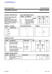
1. 54 2 54 0 9 max 3x Fig 17 SOT78 TO220AB pin 2 connected to mounting base Notes 1 Observe the general handling precautions for electrostatic discharge sensitive devices ESDs to prevent damage to MOS gate oxide 2 Refer to mounting instructions for SOT78 TO220 envelopes 3 Epoxy meets UL94 VO at 1 8 April 1998 Rev 1 100 Philips Semiconductors Product Specification PowerMOS transistor BUK453 100A B DEFINITIONS Data sheet status This data sheet contains target or goal specifications for product development This data sheet contains preliminary data supplementary data may be published later This data sheet contains final product specifications Limiting values Limiting values are given in accordance with the Absolute Maximum Rating System IEC 134 Stress above one or more of the limiting values may cause permanent damage to the device These are stress ratings only and operation of the device at these or at any other conditions above those given in the Characteristics sections of this specification is not implied Exposure to limiting values for extended periods may affect device reliability Application information Where application information is given it is advisory and does not form part of the specification Philips Electronics N V 1998 All rights are reserved Reproduction in whole or in part is prohibited without the prior written consent of the copyright owne2. O O BUK453 100AQ O O Philips Semiconductors Product Specification PowerMOS transistor BUK453 100A B GENERAL DESCRIPTION QUICK REFERENCE DATA N channel enhancement mode SYMBOL PARAMETER field effect power transistor in a sss _ oon plastic envelope BUK453 The device is intended for use in Drain source voltage Switched Mode Power Supplies Drain current DC SMPS motor control welding Total power dissipation DC DC and AC DC converters and Junction temperature in general purpose switching Drain source on state applications resistance PINNING TO220AB DESCRIPTION gate drain source drain LIMITING VALUES Limiting values in accordance with the Absolute Maximum System IEC 134 Drain source voltage 100 Drain gate voltage 100 Gate source voltage 30 100A 100B Drain current DC Drain current DC Drain current pulse peak value Total power dissipation Storage temperature Junction Temperature SYMBOL PARAMETER CONDITIONS MIN TYP MAX UNIT Thermal resistance junction to 2 K W mounting base Thermal resistance junction to K W ambient April 1998 1 Rev 1 100 Philips Semiconductors Product Specification PowerMOS transistor BUK453 100A B STATIC CHARACTERISTICS Tm 25 C unless otherwise specified Sreo panaweren __ eowomions um Ta vr Drain source breakdown Ves 0 V Ip 0 25 mA voltage Gate threshold voltage Zero gate voltage drain current Ve
3. f Vgs conditions T 25 C Vos Ves 20 40 VDS V ie 12 Typical capacitances Cs Cos Cres f Vps conditions Veg 0 V f 1 MHz Rev 1 100 Philips Semiconductors PowerMOS transistor 2 4 6 8 QG nC Fig 13 Typical turn on gate charge characteristics Vas f Q conditions I 14 A parameter Vps 0 1 VSDS V Fig 14 Typical reverse diode current l f Veps conditions Veg 0 V parameter T April 1998 Product Specification BUK453 100A B WDSS 80 100 120 140 160 180 Tmb C Fig 15 Normalised avalanche energy rating Woss f T m Conditions Ip 14 A Fig 16 Avalanche energy test circuit Wyss 0 5 LI BV yocMBV pss Vip Rev 1 100 Philips Semiconductors PowerMOS transistor MECHANICAL DATA Dimensions in mm Net Mass 2 g Product Specification BUK453 100A B 3 0 max not tinned ral max 1 2x a lt 2
4. pical output characteristics T 25 C Ip f Vps parameter Vos o DS ON Ohm 5 5 4 5 4 8 12 16 20 24 ID A Fig 6 Typical on state resistance T 25 C Foson f Ip parameter Veg Rev 1 100 Philips Semiconductors PowerMOS transistor 2 4 6 8 VGS V Fig 7 Typical pee characteristics f Vgs conditions Vps 25 V parameter T 4 8 12 16 20 24 28 ID A Fig 8 Pia transconductance T 25 C f I conditions Vps SV Normalised RDS ON f Tj 20 60 100 140 180 Tj C Fig 9 Normalised drain source on state resistance a Roson Rosonzs ce I T Ip 5A Vas 10 V April 1998 Product Specification BUK453 100A B VGS TO V J aa T 20 20 60 100 140 Tj Cc Fig 10 Gate threshold voltage Vasto f T conditions Ip 1 MA Vps Ves SUB THRESHOLD CONDUCTION 0 1 2 3 4 VGS V ms 11 Sub threshold drain current
5. r The information presented in this document does not form part of any quotation or contract it is believed to be accurate and reliable and may be changed without notice No liability will be accepted by the publisher for any consequence of its use Publication thereof does not convey nor imply any license under patent or other industrial or intellectual property rights LIFE SUPPORT APPLICATIONS These products are not designed for use in life support appliances devices or systems where malfunction of these products can be reasonably expected to result in personal injury Philips customers using or selling these products for use in such applications do so at their own risk and agree to fully indemnify Philips for any damages resulting from such improper use or sale April 1998 7 Rev 1 100
6. r Normalised Power Derating 20 40 60 80 100 120 140 160 180 Tmb C Fig 1 Normalised power dissipation PD 100 P Pp 250 F T mp Normalised Current Derating 20 40 60 80 100 120 140 160 180 Tmb C Fig 2 Normalised continuous drain current ID 100 Ip Ip 25 c I T m Conditions Veg 10 V 0 1 1 10 100 VDS V Fig 3 Safe operating area T 25 C Ip amp lom f Vos low single pulse parameter t April 1998 Product Specification BUK453 100A B Zth j mb 7 1E 02 So PEEMi ob tt tei bint tite 1E 07 1E 05 1E 03 1E 01 1E 01 t s Fig 4 Transient thermal impedance Zn j mp E t parameter D t T 10 VDS V Fig 5 Ty
7. s V Zero gate voltage drain current s V 25 C Gate source leakage current V Drain source on state BUK453 100A resistance BUK453 100B T 1 DYNAMIC CHARACTERISTICS Tmo 25 C unless otherwise specified syusot panaweren ___ eowoions um 0 Twa va sq Fone ressources v 25Vtg 5 rao fss s Cis Input capacitance Ves 0 V Vps 25 V f 1 MHz 660 825 Output capacitance A 200 Feedback capacitance 100 Turn on delay time Turn on rise time Turn off delay time Turn off fall time Internal drain inductance Measured from contact screw on tab to centre of die Internal drain inductance Measured from drain lead 6 mm from package to centre of die Internal source inductance Measured from source lead 6 mm from package to source bond pad REVERSE DIODE LIMITING VALUES AND CHARACTERISTICS Tm 25 C unless otherwise specified Sreo panaweren ___ eowpmions um rve wae or Continuous reverse drain current Pulsed reverse drain current Diode forward voltage l 14A Veas 0V 1 2 ty Reverse recovery time l 14 A dl dt 100 A us 90 ns Qr Reverse recovery charge Ves 0 V Vk 30 V 0 6 uC AVALANCHE LIMITING VALUE Tm 25 C unless otherwise specified SYMBOL PARAMETER CONDITIONS min TYP MAX UNIT Drain source non repetitive Ibp 14A Vpp lt 50V 70 mJ unclamped inductive turn off Ves 10 V Res 50 Q energy April 1998 2 Rev 1 100 Philips Semiconductors PowerMOS transisto
Download Pdf Manuals

Related Search
PHILIPS PowerMOS transistor BUK453 100A/B handbook