FAIRCHILD 74LCX10 Low Voltage Triple 3-Input NAND Gate with 5V Tolerant Inputs handbook
Contents
1. capacitance Test Switch tPLH tPHL Open 6V at Voc 3 3 03 Voc x2at Vcc 2 54 0 2V tpzutpuz GND P pxx DATA Waveform for Inverting and Non Inverting Functions CONTROL m Yee IN GND trec p CLOCK Voi teur OUTPUT Vino Vino Propagation Delay Pulse Width and trec Waveforms OUTPUT T Vee CONTROL mi oND teze teLz DATA OUT vx VoL 3 STATE Output Low Enable and Disable Times for Logic OUTPUT Vec CONTROL mi SND tPZH V DATA Woe OUT mo 3 STATE Output High Enable and Disable Times for Logic DATA IN ts CONTROL INPUT t MR OR Vmi CLEAR Setup Time Hold Time and Recovery Time for Logic Vou 90 90 10 10 VoL trise ttan FIGURE 2 Waveforms Input Characteristics f Z1MHz t t 3ns Vcc Symbol 3 3V 0 3V 2 7V 2 5V 0 2V Vmi 1 5V 1 5V Vcc 2 Vimo 1 5V 1 5V 2 Vx VoL 0 3V VoL 4 0 3V VoL 0 15V Vy Vou 0 3V Vou 0 3V Vou 0 15V www fairchildsemi com 4 Schematic Diagram Generic for LCX Family input stage www fairchildsemi com OLXO TPZ 74LCX10 Physical Dimensions inches millimeters unless otherwise 0 008 0 010 0 203 0 254 TYP ALL LEADS PLANE t 0 014 0 016 0 050 0 356 0 406 1 270 0 102 TYP ALL LEADS ALL LEAD TIPS Package Number M14A2. ALL LEADS EL e 0 335 0 344 8 509 8 738 0 228 0 244 5791 6198 7 LEAD NO 1 A IDENT 0 150 0 157 3 810 3 988 0010 0020 0 053 0 069 0 254 0 508 4 1 346 1 753j 8 MAX TYP i 9 004 0 010 0 102 0 254 0 014 0 020 0 356 0 508 0 008 1 0 203 7 REV Ay 14 Lead Small Outline Integrated Circuit SOIC JEDEC MS 012 0 150 Narrow www fairchildsemi com 6 Physical Dimensions inches millimeters unless otherwise noted Continued 10 2 0 1 1 4 TYP A mm 14 13 9 8 1 5 01 TYP 5 30 1 9 27 TYP l pee A 2 1 7 ALL LEAD TIPS PIN 1 IDENT 127 TYP 0 6 TYP LAND PATTERN RECOMMENDATION ALL LEAD TIPS D E SEE DETAIL A 8x0 ze N E E 4 0 15 0 25 DIMENSIONS ARE IN MILLIMETERS GAGE PLANE NOTES 0 8 TYP 0 25 A CONFORMS TO EIAJ EDR 7320 REGISTRATION ESTABLISHED IN DECEMBER 1998 uz B DIMENSIONS ARE IN MILLIMETERS i C DIMENSIONS ARE EXCLUSIVE OF BURRS MOLD FLASH AND TIE BAR EXTRUSIONS 0 60 0 15 SEATING PLANE M14DRevB1 DETAIL Pb Free 14 Lead Small Outline Package SOP EIAJ TYPE Il 5 3mm Wide Package Number M14D 7 www fairchildsemi com OLXO TPZ 74LCX10 Low Voltage Triple 3 Input NAND Ga
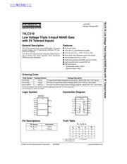
3. OO 74 CX198 FAIRCHILD a ee SEMICONDUCTOR 74LCX10 General Description tems to 3V systems CMOS low power dissipation The LCX10 contains three 3 input NAND gates The inputs tolerate voltages up to 7V allowing the interface of 5V sys The 74LCX10 is fabricated with advanced CMOS technol ogy to achieve high speed operation while maintaining June 2000 Revised February 2005 Low Voltage Triple 3 Input NAND Gate with 5V Tolerant Inputs Features E 5V tolerant inputs W 2 3V 3 6V Vcc specifications provided W 4 9 ns tpp max Vcc 3 3V 10 uA max W Power down high impedance inputs and outputs 24 mA output drive Vcc 3 0V W implements patented noise EMI reduction circuitry W Latch up performance exceeds 500 mA W ESD performance Human body model 2000V Machine model gt 200V Ordering Code Order Number Package Number Package Description 74LCX10M M14A 14 Lead Small Outline Integrated Circuit SOIC JEDEC MS 012 0 150 Narrow 74LCX10SJ M14D Pb Free 14 Lead Small Outline Package SOP EIAJ TYPE Il 5 3mm Wide 74LCX10MTC MTC14 14 Lead Thin Shrink Small Outline Package TSSOP JEDEC MO 153 4 4mm Wide Pb Free package per JEDEC J STD 020B Logic Symbol IEEE IEC Bo P 00 Co B P 0 M Ag By P 05 c Pin Descriptions Pin Names Description An Bn Cn Inputs On Outputs Devices also available in Tape and Reel Specify by
4. PRESS WRITTEN APPROVAL OF THE PRESIDENT OF FAIRCHILD SEMICONDUCTOR CORPORATION As used herein 1 Life support devices or systems are devices or systems which a are intended for surgical implant into the body or b support or sustain life and c whose failure to perform when properly used in accordance with instructions for use provided in the labeling can be rea sonably expected to result in a significant injury to the user 2 A critical component in any component of a life support device or system whose failure to perform can be rea sonably expected to cause the failure of the life support device or system or to affect its safety or effectiveness www fairchildsemi com www fairchildsemi com
5. V 2 0V Voc 3 0V 0 10 ns V Note 1 The Absolute Maximum Ratings are those values beyond which the safety of the device cannot be guaranteed The device should not be operated at these limits The parametric values defined in the Electrical Characteristics tables are not guaranteed at the Absolute Maximum Ratings The Recom mended Operating Conditions table will define the conditions for actual device operation Note 2 l5 Absolute Maximum Rating must be observed Note 3 Unused inputs must be held HIGH or LOW They may not float DC Electrical Characteristics Vec Ta 40 C to 85 C Symbol Parameter Conditions Units V Min Max HIGH Level Input Voltage 2 3 2 7 1 7 v 2 7 3 6 2 0 Vit LOW Level Input Voltage 2 3 2 7 0 7 v 2 7 8 6 0 8 Vou HIGH Level Output Voltage onu 100 uA 2 3 3 6 Voc 0 2 8 mA 23 1 8 ou 12 mA 2 7 2 2 V 18 mA 3 0 24 24 mA 3 0 22 VoL LOW Level Output Voltage oL 100 pA 2 3 3 6 0 2 oL 8mA 2 3 0 6 oL 12 mA 27 0 4 V 16 mA 3 0 0 4 24 mA 3 0 0 55 li Input Leakage Current 0 lt Vi lt 5 5V 2 3 3 6 5 0 uA lorr Power Off Leakage Current Vi or Vo 5 5V 0 10 uA loc Quiescent Supply Current Vi Voc or GND 2 3 3 6 10 3 6V lt lt 5 5V 2 3 3 6 10 as Voc 0 6V 2 3 3 6 500 www fai
6. appending the suffix letter X to the ordering code Connection Diagram Ag Bo 2 A 5 2 5 5 GND 7 Truth Table On An Bn Cn An Bn C On X X L H X X H L X X H H H H H HIGH Voltage Level X Immaterial L LOW Voltage Level 2005 Fairchild Semiconductor Corporation DS500453 www fairchildsemi com sinduj jue19 0 AG qNvN ejduj OLXO TPZ 74LCX10 Absolute Maximum 1 Symbol Parameter Value Conditions Units Voc Supply Voltage 0 5 to 7 0 V Vi DC Input Voltage 0 5 to 47 0 V Vo DC Output Voltage 0 5 to Veg 0 5 Output in HIGH or LOW State Note 2 V lik DC Input Diode Current 50 Vi lt GND mA lok DC Output Diode Current 50 Vo lt GND 50 Vo gt lo DC Output Source Sink Current 50 mA loc DC Supply Current per Supply Pin 100 mA laND DC Ground Current per Ground Pin 100 mA Tera Storage Temperature 65 to 150 Recommended Operating Conditions Note 3 Symbol Parameter Min Max Units Voc Supply Voltage Operating 2 0 3 6 Data Retention 1 5 3 6 VI Input Voltage 0 5 5 V Vo Output Voltage HIGH or LOW State 0 Voc V _ Output Current Voc 3 0V 3 6V 24 Voc 2 7V 8 0V 12 mA Voc 2 3V 2 7V 8 TA Free Air Operating Temperature 40 85 AVAV Input Edge Rate Viy 0 8
7. rchildsemi com AC Electrical Characteristics 40 C to 85 5000 Voc 3 3V 0 3V Vec 2 7V Voc 2 5V 0 2V TRUE C 50pF C 50pF C 30pF Min Max Min Max Min Max tPHL Propagation Delay 1 5 4 9 1 5 5 8 1 5 5 9 s tPLH 1 5 4 9 1 5 5 8 1 5 5 9 tosHL Output to Output Skew Note 4 1 0 losLH 1 0 Note 4 Skew is defined as the absolute value of the difference between the actual propagation delay for any two separate outputs of the same device The specification applies to any outputs switching in the same direction either HIGH to LOW tos or LOW to HIGH tosi i Dynamic Switching Characteristics Vcc 25 C Symbol Parameter Conditions Unit V Typical Voip Quiet Output Dynamic Peak VoL C 50 pF 3 3V Vi OV 3 3 0 8 C 30 pF 2 5V Vi OV 25 0 6 Quiet Output Dynamic Valley C 50 pF 3 3V Vi OV 3 3 0 8 C 30 pF 2 5V Vi OV 2 5 0 6 Capacitance Symbol Parameter Conditions Typical Units Cin Input Capacitance Voc Open OV or Vec 7 pF Cout Output Capacitance Voc 3 3V Vj OV or Voc 8 pF Cpp Power Dissipation Capacitance Voc 3 3V Vj OV or Vec f 10 MHz 25 pF 3 www fairchildsemi com OLXO TPZ 74LCX10 AC LOADING and WAVEFORMS Generic for Lcx Family FIGURE 1 AC Test Circuit C includes probe and jig
8. te with 5V Tolerant Inputs Physical Dimensions inches millimeters unless otherwise noted Continued E B ALL LEAD TIPS PIN 1 VE I DE 4 16 i i o0 42 65 4 LAND PATTERN RECOMMENDATION DETAIL A 0 09 0 20 p 200 amp BOTTOM te Max 9818 6 1 x i _ 0 10 0 05 0 65 019 0 30 0 13 a 89 05 NOTES A CONFORMS TO JEDEC REGISTRATION MO 153 VARIATION AB REF NOTE 6 DATED 7 93 B DIMENSIONS ARE IN MILLIMETERS DIMENSIONS ARE EXCLUSIVE OF BURRS MOLD FLASH AND TIE BAR EXTRUSIONS D DIMENSIONING AND TOLERANCES PER ANSI Y14 5M 1982 MTC14rcevD GAGE PLANE Un 14 Lead Thin Shrink Small Outline Package TSSOP JEDEC MO 153 4 4mm Wide Package Number MTC14 Fairchild does not assume any responsibility for use of any circuitry described no circuit patent licenses are implied and Fairchild reserves the right at any time without notice to change said circuitry and specifications LIFE SUPPORT POLICY FAIRCHILD S PRODUCTS ARE NOT AUTHORIZED FOR USE AS CRITICAL COMPONENTS IN LIFE SUPPORT DEVICES OR SYSTEMS WITHOUT THE EX
Download Pdf Manuals

Related Search
FAIRCHILD 74LCX10 Low Voltage Triple 3 Input NAND Gate with 5V Tolerant Inputs handbook