AKM AK93C85A 95A 10A 16K 32K 64Kbit Serial CMOS EEPROM
Contents
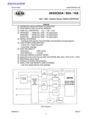
1. JA K93C 10A HH AY ASAHI KASEI AK93C85A 95A 10A AKM AK93C85A 95A 10A 16K 32K 64Kbit Serial CMOS EEPROM O0 00 OOOOO ADVANCED CMOS EEPROM TECHNOLOGY READ WRITE NON VOLATILE MEMORY WIDE VCC OPERATION Vcc 1 8V 5 5V AK93C85A 16384 bits 1024 x 16 organization AK93C95A 32768 bits 2048 x 16 organization AK93C10A 65536 bits 4096 x 16 organization SERIAL INTERFACE Interfaces with popular microcontrollers and standard microprocessors LOW POWER CONSUMPTION 0 4mA max Read Operation 0 8uA Max Standby HIGH RELIABILITY Endurance 100K cycles Data Retention 10 years Automatic address increment READ Automatic write cycle time out with auto ERASE Max 8ms VCC 4 5V 5 5V Busy Ready status signal Software controlled write protection IDEAL FOR LOW DENSITY DATA STORAGE Low cost space saving 8 pin package DAMO2E 01 DATA REGISTER Ce gt INSTRUCTION AUTO ERASE EEPROM REGISTER INSTRUCTION DECODE Gennes g3CB5A 16384bit AND P CLOCK ADD PENES 93C954 32768bit GENERATION BUFFERS i LS 93C 10A 65536bit P ed VPI GENERATOR Block Diagram 1999 10 ASAHI KASEI AK93C85A 95A 1 0A General Description The AK93C85A 95A 10A is a 16384 32768 65536 bit serial CMOS EEPROM divided into 1024 2048 4096 registers of 16 bits each The AK93C85A 95A 10A has 4 instructions such as READ WRITE EWEN and EWDS Tho2. OOXXXXXXXXXX Disables all programming instructions WRAL 1 00 01XXXXXXXXXX_ D15 D0 Writes all registers tables Instruction Set for the AK93C10A Note The WRAL instruction are used for factory function test only User can t use the WRAL instruction e The AK93C85A 95A 10A perceives the start bit in the logic 1 and also 01 DAMO2E 01 1999 10 ASAHI KASEI AK93C85A 95A 1 0A Write The write instruction is followed by 16 bits of data to be written into the specified address AK93C85A After the last bit of data is put on the DI pin the CS pin must be brought low before the next rising edge of the SK clock This falling edge of the CS initiates the self timed programming cycle The DO indicates the Busy Ready status of the chip if the CS is brought high after a minimum of 250ns Tcs AK93C95A 10A The self timed programming cycle is initiated on the rising edge of the SK clock as the last data bit DO is clocked in The DO indicates the Busy Ready status of the chip after the self timed programming cycle is initiated The Busy Ready status indicator is only valid when CS is active high When CS is low the DO output goes into a high impedance state The Busy Ready signal outputs until a start bit Logic 1 of the next instruction is given to the part DO logical 0 indicates that programming is still in progress DO logical 1 indicates that the register at the address specified in the instruc
3. Condition 4 5V lt VCC lt 5 5V 2 0V lt VCC lt 4 5V 1 8V lt VCC lt 2 0V SK Pulse Width 4 5V lt VCC lt 5 5V 2 0V lt VCC lt 4 5V 1 8V lt VCC lt 2 0V CS Setup Time CS Hold Time Data Setup Time Data Hold Time Output delay 4 5V lt VCCS5 5V 2 0V lt VCC lt 4 5V 1 8V lt VCC lt 2 0V Selftimed Programming Time 4 5V lt VCC lt 5 5V 1 8V lt VCC lt 4 5V Min CS Low Time CS to Status Valid1 CL 100pF CS to Status Valid2 CL 100pF CS to Output High Z 3 CL 100pF DAMO2E 01 2 0V lt sVCC lt 5 5V 1 8V lt VCC lt 2 0V 10 AK93C85A 95A 1 0A ASAHI KASEI AK93C85A 95A 1 0A Synchronous Data timing tCS es N tCSS tSKW tSKW tSKP LS ee x H VN WIN W DO VIZZZZZZZZAN Hi Z AK93C85A 95A 10A output a logical 1 Ready status if previous instruction is WRITE The Start of Instruction The End of Instruction DAMO2E 01 1999 10 ASAHI KASEI AK93C85A 95A 1 0A Busy Ready Signal Output AK93C95A 10A DAMO2E 01 1999 10 IMPORTANT NOTICE These products and their specifications are subject to change without notice Before considering any use or application consult the Asahi Kasei Microsystems Co Ltd AKM sales office or authorized distributor concerning their current status AKM assumes no liability for infringement of any patent intellectual property or other right in
4. the address counter rolls over to address 000 allowing the read cycle to be continued indefinitely AK93C95A When the highest address is reached 7FF the address counter rolls over to address 000 allowing the read cycle to be continued indefinitely AK93C10A When the highest address is reached FFF the address counter rolls over to address 000 allowing the read cycle to be continued indefinitely i Ay oa ZT 7 Z Z 7 j y SK o 1 2 3 4 314 Gel fal ha fa ol 30 ate Se a us 5 Z Z ore ele Z 7 Bit Code Z Z Z N Z DI eee ace ee ee o osprey 00 pos Iw G Dummy a s tt address A9 AO address A9 AQ 1 x l AK93C85A output a logic 1 Ready stat if previous instruction is WRITE READ AK93C85A S 4 CS 2 Z Z Z7 Ll i j Z Z SK 0 1 2 3 4 5 7 13 fial hs fie y Bol fai h 48 7 Z WA AA 7 DI o Fr lee 7 7 Start Op Z Z Z Bit ode Z 7 Z Z DO Sa E 7 o Pepe Te Pel ZT k 4 De Oe Se ee AK93C95A output a logic 1 Ready status bit address A10 A0 address A10 A0 1 if previous instruction is WRITE READ AK93C95A Ay cS Go ae a j A Z AAR RAR RR RAR SK 0 1 2 3 4 5 14 hs fie 117 Z 31 32 7 47 Z A Z Z Z Z DI o fi 7 Le Ma 7 7 TEA 5 Start og 4 Z Z Bit ode Z Z Z A 4 7 DO a tt 1 o nis na Z roms A ummy a sae E peer eo output a logic 1 Ready status bit address A11 A0 address A11 A0j 1 if previous instruction i
5. the application or use of any information contained herein Any export of these products or devices or systems containing them may require an export license or other official approval under the law and regulations of the country of export pertaining to customs and tariffs currency exchange or strategic materials AKM products are neither intended nor authorized for use as critical components in any safety life support or other hazard related device or system and AKM assumes no responsibility relating to any such use except with the express written consent of the Representative Director of AKM As used here a A hazard related device or system is one designed or intended for life support or maintenance of safety or for applications in medicine aerospace nuclear energy or other fields in which its failure to function or perform may reasonably be expected to result in loss of life or in significant injury or damage to person or property b A critical component is one whose failure to function or perform may reasonably be expected to result whether directly or indirectly in the loss of the safety or effectiveness of the device or system containing it and which must therefore meet very high standards of performance and reliability lt is the responsibility of the buyer or distributor of an AKM product who distributes disposes of or otherwise places the product with a third party to notify that party in advance of the above content a
6. alling edge of the CS initiates the self timed programming cycle the DO indicates the Busy Ready status of the chip if the CS is brought high after a minimum of 250ns Tcs DO logical 0 indicates that programming is still in progress DO logical 1 indicates that the register at the address specified in the instruction has been written with the new data pattern contained in the instruction and the part is ready for a next instruction The Busy Ready status indicator is only valid when CS is active high When CS is low the DO output goes into a high impedance state The Busy Ready signal outputs until a start bit Logic 1 of the next instruction is given to the part E Type of Products Model Memory size Temp Range Vcc Package AK93C85AF 16Kbits 40 C 85 C 1 8V 5 5V 8pin Plastic SOP AK93C85AM 40 C 85 C 1 8V 5 5V 8pin Plastic SSOP AK93C95AF 32Kbits 40 C 85 C 1 8V 5 5V 8pin Plastic SOP AK93C10AF 64Kbits 40 C 85 C 1 8V 5 5V 8pin Plastic SOP DAMO2E 01 1999 10 ASAHI KASEI AK93C85A 95A 1 0A Pin arrangement AK93C85AF AK93C85AM NC vcc CS SK 8pin SOP AK93C95AF 10AF 8pin SSOP 8pin SOP Pin Name Function CS Chip Select SK Serial Data Clock DI Serial Data Input DO Serial Data Output GND Ground Vcc Power Supply NC Not Connected DAMO2E 01 1999 10 ASAHI KASEI AK93C85A 95A 1 0A Functional Description The AK93C85A 95A 10A has 4 in
7. device This is a stress rating only and functional operation of the device at these or any other conditions above those indicated in the operational sections of the specification is not implied Exposure to absolute maximum conditions for extended periods may affect device reliability Recommended Operating Condition Symbol Power Supply VCC 1 8 5 5 V Ambient Operating Temperature Ta 40 85 C DAMO2E 01 1999 10 ASAHI KASEI AK93C85A 95A 1 0A Electrical Characteristics 1 D C ELECTRICAL CHARACTERISTICS 1 8V lt Vcc lt 5 5V 40 C lt Ta lt 85 C unless otherwise specified Parameter Symbol Condition Current Dissipation VCC 5 5V tSKP 1us 5 5 WRITE VCC 1 8V tSKP 4us 3 0 Current Dissipation VCC 5 5V tSKP 1us 0 4 READ EWEN EWDS VCC 1 8V tSKP 4us 0 1 Current Dissipation VCC 5 5V 0 8 Standby Input High Voltage 0 8 x VCC VCC 0 5 Input Low Voltage 0 1 0 2 x VCC Output High Voltage 2 5V lt VCC lt 5 5V 0 8 x VCC IOH 0 1mA 1 8V lt VCC lt 2 5V 0 8 x VCC IOH 0 1mA Output Low Voltage 2 5V lt VCC lt 5 5V IOL 1 0mA 1 8V lt VCC lt 2 5V IOL 0 1mA Input Leakage VCC 5 5V VIN 5 5V Output Leakage VCC 5 5V VOUT 5 5V CS GND 1 VIN VIH VIL DO Open 2 VIN VCC GND CS GND DO Open DAMO2E 01 1999 10 ASAHI KASEI 2 A C ELECTRICAL CHARACTERISTICS Parameter SK Cycle Time Symbol 1 8V lt Vcc lt 5 5V 40 C lt Ta lt 85 C unless otherwise specified
8. nd conditions and the buyer or distributor agrees to assume any and all responsibility and liability for and hold AKM harmless from any and all claims arising from the use of said product in the absence of such notification
9. s WRITE bof READ AK93C10A DAMO2E 01 1999 10 ASAHI KASEI AK93C85A 95A 1 0A EWEN EWDS When Vcc is applied to the part the part automatically powers up in the ERASE WRITE Disable state In the ERASE WRITE disable state execution of WRITE instruction is disable Before WRITE instruction is executed EWEN instruction must be executed The ERASE WRITE enable state continues until EWDS instruction is executed or Vcc is removed from the part Execution of a read instruction is independent of both EWEN and EWDS instructions SSS S K 0 1 2 3 4 5 6 7 8 9 fro foal pel jis EWEN 11 Start EWDS 00 Bit D 0 High Z AK93C85A output a logic 1 Ready status 7 if previous instruction is WRITE X Dont care EWEN EWDS AK93C85A SSS SSS SK oj fil fel Jak Jal js JelL 7LH8lL olhol hill h2 hs Na DI o EWEN 11 Start EWDS 00 D 0 cS High 2 AK93C95A output a logic 1 Ready status E ee X Don t care if previous instruction is WRITE EWEN EWDS AK93C95A Start EWDS 00 D High Z 0 AK93C10A output a logic 1 Ready status if previous instruction is WRITE X Dont care EWEN EWDS AK93C10A DAMO2E 01 1999 10 ASAHI KASEI AK93C85A 95A 1 0A Absolute Maximum Ratings Parameter Power Supply 7 0 All Input Voltages VCC 0 6 with Respect to Ground Ambient storage temperature 150 Stress above those listed under Absolute Maximum Ratings may cause permanent damage to the
10. se instructions control the AK93C85A 95A 10A The AK93C85A 95A 10A can operate full function under wide operating voltage range from 1 8V to 5 5V The charge up circuit is integrated for high voltage generation that is used for write operation A serial interface of AK93C85A 95A 10A consisting of chip select CS serial clock SK data in DI and data out DO can easily be controlled by popular microcontrollers or standard microprocessors AK93C85A 95A 10A takes in the write data from data input pin DI to a register synchronously with rising edge of input pulse of serial clock pin SK And at read operation AK93C85A 95A 10A takes out the read data from a register to data output pin DO synchronously with rising edge of SK The DO pin is usually in high impedance state The DO pin outputs L or H in case of data output or Busy Ready signal output Software controlled write protection When Vcc is applied to the part the part automatically powers up in the ERASE WRITE Disable state In the ERASE WRITE disable state execution of WRITE instruction is disabled Before WRITE instruction is executed EWEN instruction must be executed The ERASE WRITE enable state continues until EWDS instruction is executed or Vcc is removed from the part Execution of a read instruction is independent of both EWEN and EWDS instructions Busy Ready status signal After a write instruction the DO output serves as a Busy Ready status indicator After the f
11. structions such as READ WRITE EWEN and EWDS A valid instruction consists of a Start Bit Logic 1 the appropriate Op Code and the desired memory Address location The CS pin must be brought low for a minimum of 250ns Tcs between each instruction when the instruction is continuously executed Instruc Start Op Address Data Comments tion Bit Code READ 1 10 A9 A0 D15 D0 Reads data stored in memory at specified address WRITE 1 01 A9 A0 D15 D0 Writes register EWEN 1 00 11XXXXXXXX Write enable must precede all programming modes EWDS 1 00 O0OXXXXXXXX Disables all programming instructions WRAL 1 00 01XXXXXXXX D15 D0 Writes all registers tablet Instruction Set for the AK93C85A Instruc Start Op Address Data Comments tion Bit Code READ 1 10 A10 A0 D15 D0 Reads data stored in memory at specified address WRITE 1 01 A10 A0 D15 D0 Writes register EWEN 1 00 11XXXXXXXXX Write enable must precede all programming modes EWDS 1 00 OOXXXXXXXXX Disables all programming instructions WRAL 1 00 01XXXXXXXXX D15 D0 Writes all registers table2 Instruction Set for the AK93C95A Instruc Start Op Address Data Comments tion Bit Code READ 1 10 A11 A0 D15 D0 Reads data stored in memory at specified address WRITE 1 01 A11 A0 D15 D0 Writes register EWEN 1 00 11XXXXXXXXXX Write enable must precede all programming modes EWDS 1 00
12. tion has been written with the new data pattern contained in the instruction and the part is ready for a next instruction 4 Y Z a O Y SK 0 1 2 3 4 5 A 12 fis fe AZ A i Y f DI o FL M eE A 7 Ne ea ee EET a A Z S Bae Z A i Le A ee DO EL High Z GY Yy a i AK93C85A output a logic Ready status tE if previous instruction is WRITE WRITE AK93C85A Z Le 3 cs J f 7 g S K 0 E a 3 4 5 A 13 la 15 16 Z A Y DI Le TE CEE De roi Z rk Code h Y DO a iat 2 J _ _ 7 S AK93C95A output a logic 1 Ready status tE if previous instruction is WRITE WRITE AK93C95A ae 7 yo f Y G SK 0 1 2 3 4 5 h 14 ps 16 17 h y DI of Le ig SEN E E EN ED WZ f or Bode Ye g Y DO cess eR 1 7 Y Ap ewe 7 WRITE AK93C10A DAMO2E 01 1999 10 ASAHI KASEI AK93C85A 95A 1 0A Read The read instruction is the only instruction which outputs serial data on the DO pin Following the Start bit first Op code and address are decoded then the data from the selected memory location is available at the DO pin A dummy bit logical 0 precedes the 16 bit data from the selected memory location The output data changes are synchronized with the rising edges of the serial clock Sk The data in the next address can be read sequentially by continuing to provide clock The address automatically cycles to the next higher address after the 16bit data shifted out AK93C85A When the highest address is reached 3FF
Download Pdf Manuals

Related Search
AKM AK93C85A 95A 10A 16K 32K 64Kbit Serial CMOS EEPROM