ZETEX ZXT2M322 Data sheet
Contents
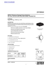
1. zZ 00m 10m 100m 1 10m 100m 1 Collector Current A Collector Current A he vl Vogsan V lc 1 0 0 8 0 6 0 4 02m 10m 100m 1 Collector Current A V on V lc ZETEX ZXT2M322 MLP322 PACKAGE OUTLINE 2mm x 2mm Micro Leaded Package x4 sides SEATING PLANE MILLIMETRES CONTROLLING DIMENSIONS IN MILLIMETRES APPROX CONVERTED DIMENSIONS IN INCHES PACKAGE DIMENSIONS INCHES MILLIMETRES EXPOSED PAD INCHES MIN MAX MIN MAX MIN MAX MIN MAX 0 80 1 00 0 0315 0 0393 0 65 REF 0 0255 REF Zetex plc 2002 Europe Zetex plc Fields New Road Chadderton Oldham OL9 8NP United Kingdom Telephone 44 161 622 4422 Fax 44 161 622 4420 uksales zetex com Zetex GmbH StreitfeldstraRe 19 D 81673 M nchen Germany Telefon 49 89 45 49 49 0 Fax 49 89 45 49 49 49 europe sales 2zetex com Americas Zetex Inc 700 Veterans Memorial Hwy Hauppauge NY117882. 258ZXT2M 32244 Ny FH ZXT2M322 MPPS Miniature Package Power Solutions 20V PNP LOW SATURATION SWITCHING TRANSISTOR SUMMARY VcEo 20V Rsat 64mQ Ic 3 5A DESCRIPTION Packaged in the innovative 2mm x 2mm MLP Micro Leaded Package outline this new 4 generation low saturation transistors offers extremely low on state losses making it ideal for use in DC DC circuits and various driving and power management functions Additionally users will also gain several other key benefits Performance capability equivalent to much larger packages 2mm x 2mm MLP single die Improved circuit efficiency amp power levels Lower package height nom 0 9mm PCB area and device placement savings Reduced component count FEATURES e Low Equivalent On Resistance e Extremely Low Saturation Voltage 220mV 1A e hee characterised up to 6A e c 3 5A Continuous Collector Current e 2mm x 2mm MLP APPLICATIONS e DC DC Converters FET Drivers e Charging Circuits e Power switches PINOUT e Motor control ORDERING INFORMATION LJ DEVICE QUANTITY PER REEL ZXT2M322TA 3000 ZXT2M322TC 10000 DEVICE MARKING 2mm x 2mm Single MLP S2 underside view ZXT2M322 ABSOLUTE MAXIMUM RATINGS PARAMETER SYMBOL Collector Base Voltage VcBO Collector Emitter Voltage Emitter Base Voltage Peak Pulse Current c Continuous Collector Current a Base Current P
3. BO V BR CEO Ic 100nA Ic 10mA Emitter Base Breakdown Voltage V BR EBO Ip 100nA Collector Cut Off Current IcBo Vcp 20V Emitter Cut Off Current lEBO Vep 6V Collector Emitter Cut Off Current ICES Vces 16V Collector Emitter Saturation Voltage VcE sat Ic 0 1A Ip 10mA Ic 1A Ig2 20mA Ic 1 5A lp 50mA Ic 2 5A Ig 150mA Ic 3 5A Ig 350mA Base Emitter Saturation Voltage VBE sat Ic 3 5A Ig 350mA Base Emitter Turn On Voltage VBE on Ic 3 5A Vcg 2V Static Forward Current Transfer Ratio hrE Ic2 10mA Vcg 2V Ic 0 1A Vcg 2V Ic 2A Vcg 2V Ic 6A Vcg 2V Transition Frequency Ic 50mA Vcg 10V f 100MHz Output Capacitance Vop 10V f 1MHz Turn On Time Turn Off Time Vec 10V Ic 1A Ig421g2210mA Measured under pulsed conditions Pulse width 300us Duty cycle lt 2 ISSUE 2 JUNE 2002 ZETEX ZXT2M322 CHARACTERISTICS 10m 100m 1 D pe 10m 100m 1 Collector Current A Collector Current A Vesan v lc Vesan id lc 14 12 1 0 0 8 0 6 0 4 0 2
4. USA Telephone 631 360 2222 Fax 631 360 8222 usa sales zetex com These offices are supported by agents and distributors in major countries world wide Asia Pacific Zetex Asia Ltd 3701 04 Metroplaza Tower 1 Hing Fong Road Kwai Fong Hong Kong Telephone 852 26100 611 Fax 852 24250 494 asia sales zetex com This publication is issued to provide outline information only which unless agreed by the Company in writing may not be used applied or reproduced for any purpose or form part of any order or contract or be regarded as a representation relating to the products or services concerned The Company reserves t For the latest product information log on to WWW zetex com ZETEX e right to alter without notice the specification design price or conditions of supply of any product or service ISSUE 2 JUNE 2002
5. of Ptot 420mW ZETEX ZXT2M322 Collector Current A Single Pulse T 25 C 1 10 50 75 100 125 150 V Collector Emitter Voltage V Temperature C Safe Operating Area Derating Curve Max Power Dissipation VW z6 0 0 7 20 EN d 8 E oO Thermal Resistance C W 20z copper fou 1m 10m 100m 1 10 Qa 1 10 100 Pulse Width s Board Cu Area sqcm Thermal Resistance v Board Area Dissipation W P m n 001 1 Board Cu Area sqcm Power Dissipation v Board Area ZETEX ZXT2M322 ELECTRICAL CHARACTERISTICS at T 25 C unless otherwise stated PARAMETER SYMBOL CONDITIONS Collector Base Breakdown Voltage Collector Emitter Breakdown Voltage V BR C
6. ower Dissipation at TA 25 C a Linear Derating Factor Power Dissipation at TA 25 C b Linear Derating Factor Power Dissipation at TA 25 C d Linear Derating Factor Power Dissipation at TA 25 C e Linear Derating Factor Operating and Storage Temperature Range 55 to 150 THERMAL RESISTANCE PARAMETER SYMBOL Junction to Ambient a RoJA Junction to Ambient b RoJA Junction to Ambient d ReJA Junction to Ambient e RJA NOTES a For a single device surface mounted on 10sq cm10z copper on FR4 PCB in still air conditions with all exposed pads attached b For a single device surface mounted on 10sq cm10z copper on FR4 PCB in still air conditions measured at t lt 5 secs with all exposed pads attached c Repetitive rating pulse width limited by max junction temperature refer to Transient Thermal Impedance graph d For a single device surface mounted on 10sq cm10z copper on FR4 PCB in still air conditions with minimal lead connections only e For a single device surface mounted on 65sq cm2oz copper on FR4 PCB in still air conditions with all exposed pads attached f The minimum copper dimensions required for mounting are no smaller than the exposed metal pads on the base of the device as shown in the package dimensions data The thermal resistance for a device mounted on 1 5mm thick FR4 board using minimum copper of 10z weight is Rth 300 C W giving a power rating
Download Pdf Manuals

Related Search
ZETEX ZXT2M322 Data sheet