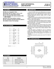
Micrel QUINT DIFFERENTIAL LINE RECEIVER SY10E116 SY100E116 Manual
Contents
1. AC ELECTRICAL CHARACTERISTICS VEE VEE Min to VEE Max Vcc VCco GND Ta 40 C Ta 25 C Ta 85 C symbol Parameter Iw Typ Max win Typ Max Min Typ max win Typ max Propagation Delay to ps Output D 150 300 500 200 300 450 200 300 450 200 300 450 D S E 150 300 550 150 300 500 150 200 500 150 300 500 voo inputSenitviy 150 150 150 150 150 mw tskew Within Device Skew 50 50 50 50 ps Dn to Qn Qn tskew Duty Cycle Skew 10 10 10 10 ps tPLH tPHL tr Rise Fall Time 250 375 625 275 375 575 275 375 575 275 375 575 ps tf 20 to 80 NOTES 1 Minimum input swing for which AC parameters are guaranteed 2 Within device skew is defined as identical transitions on similar paths through a device 3 Duty cycle skew is defined only for differential operation when the delays are measured from the cross point of the inputs to the cross point of the outputs PRODUCT ORDERING CODE Ordering Package Operating Ordering Package Operating Code Type Range Code Type Range SY100E116JCTR J28 1 SY100E116JITR J28 1 SY10E116 Micrel SY100E116 28 LEAD PLCC J28 TOP VIEW SIDE 0 048 1 22 Ze 0 042 1 07 SEE DETAIL A 0 048 1 22 BOTTOM VIEW 0 0422. 1 07 ee KN i 1 r fami S Es N De dei LTL VA O R iN Km duU i Kat ks J i fey E 0 490 22088 E Sebel 1 7 T ZEN 12 454813 ADD a E m ei e a zl CL 2 0 452908 O H ad 11 48388 O H E cA o g ES an t KR SSS Lr Lr Se tooo AA Ce LG A 1878 0 49078 008 a 0 004 0 10 12 452213 ES P NOTES 1 DIMENSIONS ARE IN INCHES MM 2 CONTROLLING DIMENSION INCHES A DIMENSION DOES NOT INCLUDE MOLD FLASH OR PROTRUSIONS EITHER OF WHICH SHALL NOT EXCEED 0 008 0 203 l i A LEAD DIMENSION DOES NOT INCLUDE DAMBAR 5 PROTRUSION A Leg 0 462213 0 020 0 51 MIN MAXIMUM AND MINIMUM SPECIFICATIONS AR INDICATED AS FOLLOWS MAX MIN 0 101 8001 2 56 5 2 t PACKAGE TOP DIMENSION MAY BE SLIGHTLY SMALLER THAN BOTTOM DIMENSION 0 050 1 27 Ka BSC JIL 0 032f0 81J A 0 026 0 66 as Rev 03 DETAIL A SY10E116 Micrel SY100E116 MICREL SYNERGY 3250SCOTT BOULEVARD SANTACLARA CA95054 USA TEL 1 408 980 9191 Fax 1 408 914 7878 wes http www micrel com This information is believed to be accurate and reliable however no responsibility is assumed by Micrel for its use nor for any infringement of patents or other rights of third parties resulting from its use No license is granted by implication or otherwise under any patent or patent right of Micrel Inc 2000 Micrel Incorporated 4
3. ZIT 341 C e a re MICHEL The Infinite Bandwidth Company FEATURES E 450ps max Propagation Delay E Extended 100E VEE range of 4 2V to 5 5V E VBB output for single ended reception E Fully compatible with industry standard 10KH 100K I O levels E Internal 75KQ input pulldown resistors E Fully compatible with Motorola MC10E 100E116 E Available in 28 pin PLCC package BLOCK DIAGRAM Do Qo Do I gt Qo D1 Qi Di IJ Qi D2 Q2 D2 d Q2 D3 Q3 D3 IJ Q3 D4 Q4 D4 IJ Q4 Pn O Function Do Do D4 D4 Differential Input Pairs Qo Qo Q4 Q4 Differential Output Pairs Reference Voltage Output Vcc to Output QUINT DIFFERENTIAL LINE RECEIVER SY10E116 SY100E116 DESCRIPTION The SY10 100E116 are quint differential line receivers designed for use in new high performance ECL systems These devices have emitter follower outputs and an internally generated reference supply VBB for single ended reception Active current sources combined with Micrel Synergy s ASSET technology provide the receivers with excellent common mode noise rejection The receiver design features clamp circuitry to cause a defined output state if both the inverting and non inverting inputs are left open in this case the Q output goes LOW while the Q output goes HIGH If both inverting and non inverting inputs are at equal potential the receiver does not go to a defined state but rather shares c
4. urrent in normal differential amplifier fashion producing output voltage levels midway between HIGH and LOW The VBB output is intended for use as a reference voltage for single ended reception of ECL signals to that device only When using VBB for this purpose it is recommended that VBB is decoupled to Vcc via a 0 01 uF capacitor For higher bandwidth please refer to the SY10 100E416 device PIN CONFIGURATION Q Q oO OO SO OS 25 24 23 22 21 20 19 Ds 26 18 Q3 D2 27 17 Q3 D2 28 PLCC 16 Vcc VEE O TOP VIEW 15 Q2 VBB 2 J28 1 14 Q2 Do 3 13 Vcco Do 4 120771 Q1 5 6 7 8 9101 Soe Ge e O gt gt Rev E Issue Date November 1998 Amendment 0 SY10E116 Micrel SY100E116 LOGIC EQUATION Qn Dn DC ELECTRICAL CHARACTERISTICS VEE VEE Min to VEE Max Vcc Vcco GND Output Reference Voltage in Input HIGH Current VBB IIH IEE DC Input Sensitivity 150 Common Mode Range 2 0 NOTES 1 VPP is the minimum differential input voltage required to assure full ECL levels are present at the outputs 2 Vcomp is referenced to the most positive side of the differential input signal Normal operation is obtained when the HIGH input is within the Vcmr range and the input swing is greater than Vpp min and lt 1V
Download Pdf Manuals

Related Search
Micrel QUINT DIFFERENTIAL LINE RECEIVER SY10E116 SY100E116 Manual