ANALOG DEVICES AD6623handbookRev A
Contents
1. EE KEY ROSS 28 Driving Multiple TSP Serial Ports 43 Output Clip Detection 1e amara ted cn OE REA deta eigene 28 USING THE AD6623 TO PROCESS TWO UMTS CARRIERS Cascading Multiple AD66238 28 WITH 24 OUTPUT RATE Ts oo Ran CEDERE QUEM 44 Selection of Real and Complex Data Types 29 DUOSTVIE ue css A SEN Le RT pam eben QA ATE 44 SYNCHRONIZATION orenean EEEN TE i m hn 29 Configuring the AD6623 44 Hold Off Counters and Shadow Registers 29 AD6623 Register Configuration 44 Start d RR eec og Suen a te Ee en eee 29 THERMAL MANAGEMENT 0000 cee n 46 Start with No Syne vies wer e eph RUE RENAL n 29 OUTLINE DIMENSIONS s esses ee 47 Revision HOR Pe Se nd wae ene AMER ee qe 48 2 REV A AD6623 PRODUCT DESCRIPTION The AD6623 is a 4 channel Transmit Signal Processor TSP that creates high bandwidth data for Transmit Digital to Analog Converters TxDACs from baseband data provided by a Digi tal Signal Processor DSP Modern TxDACs have achieved sufficiently high sampling rates analog bandwidth and dynamic range to create the first Intermediate Frequency IF directly The AD6623 synthesizes multicarrier and multistandard di2. aos eset o Ste seed 39 PROGRAMMABLE RAM COEFFICIENT FILTER RCF 16 0xn02 NCO Frequency eerie eee eect ae 39 OVERVIEW OF THE RCF BLOCKS 17 0xn03 NCO Frequency Update Hold Off Counter 39 INTERPOLATING FIR FILTER 18 0xn04 NCO Phase 39 Channel RCF Control Registers 20 0xn05 NCO Phase Offset Update Hold Off Counter 39 PSK MODULATOR Exe EE Dane ee Me 20 02006 CIC Scale ees agente dit aren eee 39 TA A DOSPK Modulation 21 0xn07 CIC2 Decimation 1 1 39 8 PSK Modulation r a ayunaspa pupas eee nee 21 0xn08 CIC2 Interpolation 1 Leica 1 39 30 8 8 PSK Modulation 21 0509 CICS Interpolation Dee es 39 MSE Look Up Table ES RR UE 22 0xn0A Number of RCF Coefficients 1 39 GMSK Look Up Table serok Rau CREER ad AK 22 0xn0B RCF Coefficient Offset 39 OPSK Look Up Table iz 9 ei hand Foe Oo ERA REY RAP 22 0xn0C Channel Mode Control 1 39 PHASE EQUALIZER a aaa quas ka baha aen AS
3. 0 1000 2000 3000 4000 5000 6000 7000 8000 9000 10000 kHz Figure 44 RCF and CIC Frequency Response for WBCDMA USING THE AD6623 TO PROCESS TWO UMTS CARRIERS WITH 24x OUTPUT RATE Overview The AD6623 may be used to process two UMTS carriers each with an output rate of 24x i e 92 16 MSPS The AD6623 configuration used to accomplish this consists of using two pro cessing channels in parallel to process each UMTS carrier The ideology behind the parallel processing approach is that each channel operates on half of the input samples processing every other sample The reason is that the serial input data rate is limited to 3 25 MSPS for 16 bit I and 16 bit Q data 104 MSPS 32 The first channel of each pair begins processing the first input sample immediately The second channel begins processing after a specific delay so that the two channels essentially will be operating 180 degrees out of phase with each other Since each channel processes only half the input samples and thus receives input data at half the original rate each channel has twice the original amount of time available for processing This in turn makes available twice the original number of taps resulting in much improved digital filtering capability To maximize the number of available FIR filter taps the highest possible input rate should be used 44 Therefore this application note assumes an input sample rate of 3 84
4. 21 The pass band droop of CIC5 should be calculated using this equation and can be compensated for in the RCF stage The gain should be calculated from the CIC scaling section above Programming Guidelines for AD6623 CIC Filters The values M cico 1 2 1 can be independently pro grammed for each channel at locations 0xn07 0xn08 While these control registers are nine bits and 12 bits wide respec tively M cic 1 and L crc2 1 should be confined to the ranges shown by Table XIII according to the interpolation factor of the CIC5 Exceeding the recommended guidelines may result in overflow for input sequences at or near full scale While rela tively large ratios of L cic M cic allow for the larger overall interpolations with minimal power consumption 2 should be minimized to achieve the best overall image rejection 26 As an example consider an input from the CIC5 whose bandwidth is 0 0033 of the CIC5 rate centered at baseband Interpolation by a factor of five reveals five images as shown below 10 dB 4 3 2 1 0 1 2 3 Figure 31 Unfiltered rCIC2 Images The rCIC2 rejects each of the undesired images while passing the image at baseband The images of a pure tone at channel center DC are nulled perfectly but as the bandwidth increases the rejection is diminished The lower band edge of the first image always has the least rejection In this example the rCI
5. 0 3 V to 5 V 5 V Tolerant Output Voltage Swing 0 3 V to VDDIO 0 3 V Load Capacitance 200 pF Junction Temperature Under Bias 125 C Operating Temperature 40 C to 85 C Ambient Storage Temperature Range 65 C to 150 C Lead Temperature 5 sec 280 Stresses greater than those listed above may cause permanent damage to the device These are stress ratings only functional operation of the devices at these or any other conditions greater than those indicated in the operational sections of this specification is not implied Exposure to absolute maximum rating conditions for extended periods may affect device reliability THERMAL CHARACTERISTICS 128 Lead MQFP with Internal Heat Spreader 28 1 C W no airflow 22 6 C W 200 airflow 20 5 C W 400 lfpm airflow 196 Lead BGA 6j4 26 3 C W no airflow O14 22 C W 200 Ifpm airflow Thermal measurements made in the horizontal position on a 4 layer board EXPLANATION OF TEST LEVELS I 100 Production Tested II 100 Production Tested at 25 C and Sample Tested at Specified Temperatures III Sample Tested Only IV Parameter Guaranteed by Design and Analysis V Parameter is Typical Value Only ORDERING GUIDE Model Temperature Range Package Description Package Option AD6623AS 40 C to 85 C Ambient 128 Lead MQFP
6. OSS 7 aed Sneed em MOX ERAS 33 ABSOLUTE MAXIMUM RATINGS 10 Mu lticarnier Scalig oes vv y SESE ae ECKE RW 33 THERMAL CHARACTERISTICS 10 Single Carrier Scalig sese ek EC 33 EXPLANATION OF TEST LEVELS 10 MICROPORT INTERFACE 34 ORDERING GUIDE PAE E 10 Micr port Control isisa ae aulas pacte ERE E a RR eet 34 PIN CONFIGURATION 128 Lead MQFP 11 EXTERNAL MEMORY MAP 34 128 PIN FUNCTION DESCRIPTION 12 Intel Nonmultiplexed Mode INM 35 PIN CONFIGURATION 196 Lead CSPBGA 13 Motorola Nonmultiplexed Mode 35 196 PIN FUNCTION DESCRIPTION 14 External Address 7 Upper Address Register UAR 35 POWERSUPPLY s taa T dre NU RU QU nda PAN 14 External Address 6 Lower Address Register LAR 35 INPUTS cee Re oak Sei es PE heen RR MERE CoS 14 External Address 5 35 CONTROL ee we nena REY 14 External Address 4 Sleep eS ee XY x AS 36
7. Switching Characteristics sciri TCLK to TSCLK Delay divide by 1 Full IV 4 10 5 ns tpscLKH TCLK to TSCLK Delay for any other divisor Full IV 5 13 ns tDSCLKL TCLK to J SCLK Delay divide by 2 or even number Full IV 3 5 9 ns tpscLKLL CLK to Delay divide by 3 or odd number Full IV 4 10 ns Channel is Self Framing tssDIo SDIN to TSCLK Setup Time Full IV 1 7 ns SDIN to TSCLK Hold Time Full IV 0 ns tpsEO0A TSCLK to SDFO Delay Full IV 0 5 3 5 05 Channel is External Framing tssFIO SDFI to TSCLK Setup Time Full IV 2 ns THSFIO SDFI to SCLK Hold Time Full IV 0 05 15800 SDIN to TSCLK Setup Time Full IV 2 ns tHSDIO SDIN to TSCLK Hold Time Full IV 0 ns tpsFooB TSCLK to SDFO Delay Full IV 0 5 3 ns Slave Mode Serial Port Timing Requirements SCS 1 Switching Characteristics SCLK Period Full IV 2 X terx ns tscLKL SCLK Low Time Full IV 3 5 ns tscLKH SCLK High Time Full IV 3 5 ns Channel is Self Framing tsspH SDIN to TSCLK Setup Time Full IV 1 ns tyspH SDIN to TSCLK Hold Time Full IV 2 5 ns tpsFo1 TSCLK to SDFO Delay Full IV 4 10 ns Channel is External Framing tssEI SDFI to TSCLK Setup Time Full IV 2 ns SDFI to TSCLK Hold Time Full IV 1 ns SDIN TSCLK Setup Time Full IV 1 ns SDIN to TSCLK Hold Time Full IV 2 5 ns tpsFo1 to SDFO Delay Full IV 10 ns NOTES All Timing Specifications valid over VDD range of 2 375 V to 2 675 V and VDDIO range of 3 0 V to 3 6 V 2Croap
8. The ramp unit when bypassed will have exactly 0 dB of gain and can be ignored When in use the gain is dependant on what value 15 stored in the last valid RMEM location RMEM words are 14 bits 0 1 so when the value is positive full scale the gain is about 0 0005 dB probably neglectable The RCF coefficients should be normalized to positive full scale This will yield the greatest dynamic range The RCF is equipped with an output scaler that ranges from 0 dB to 18 06 dB below full scale in 6 02 dB steps This attenuation can be used par tially compensate for filter gain in the RCF For example if the maximum gain of the RCF coefficients is 11 26 dB the RCF coarse scale should be set to 2 12 04 dB This yields an RCF output level and fine scale input level of 0 78 dB 11 26 12 04 0 78 24 The fine scale unit is left to turn 0 78 dB level into a 5 59 dB level This requires a gain of 4 81 dB which corresponds to a 14 bit 0 2 scale value of 1264h All subsequent rescalings during chip operation should be relative to this maximum 5 59 0 78 4 81 25 481 floor ho 2 x 12644 26 Finally as described in the RCF section there may be a worst case peak of a phase that is larger than the channel center gain In the preceding example if the worst case to channel center ratio is larger than 4 59 dB potentially overflowing the RCF then the RCF_ Coarse Scale should be reduced by one and the CIC S
9. Bit 3 Reserved Bit 2 High enables Serial Time Slot Syncs not available in FIR Mode Bit 1 High enables Power Ramp coefficient interpolation Bit 0 High enables the Power Ramp 40 0xn17 Power Ramp Length 0 This is the length of the ramp for Mode 0 minus one 0xn18 Power Ramp Length 1 This is the length of the ramp for Mode 1 minus one Setting this to zero disables dual ramps 0xn19 Power Ramp Rest Time This is the number of RCF output samples to rest for between ramp down and a ramp up 0xn1A 0xn1F Unused 0xn20 0xn3F Data Memory This group of registers contain the RCF Filter Data See the RCF section for additional details 0xn40 0xn7F Power Ramp Coefficient Memory This group of registers contain the Power Ramp Coefficients See the Power Ramp section for additional details 0xn80 0xnFF Coefficient Memory This group of registers contain the RCF Filter Coefficients See the RCF section for additional details PSEUDOCODE Write Pseudocode Void Write Micro ext address int data Main This code shows the programming of the NCO frequency register using the Write Micro function defined above The variable address is the External Address A 2 0 and data is the value to be placed in the external interface register Internal Address 0x102 channel 1 Holding registers for NCO byte wide access data int d3 d2 d1 d0 word CO_FREQ 0x1BEFEFFF write Chan rite
10. Ch A RCF Phase EQ Coef2 0x112 16 15 0 Ch A RCF MPSK Magnitude 0 0 113 16 15 0 Ch RCF Magnitude 1 0 114 16 15 0 Ch RCF Magnitude 2 0 115 16 15 0 Ch RCF Magnitude 3 0 116 8 7 Reserved 6 Ch A Serial Data Frame Select 0 Serial Data Frame Request 1 Serial Data Frame End 20 Figure 21 16 Phase Modulations REV A AD6623 All of these phase locations are represented in rectangular coor dinates by only four unique magnitudes in the positive and negative directions These four values are read from four channel registers that are programmed according to the following table which gives the generic formulas and a specific example The example is notable because it is only 0 046 dB below full scale and the 16 bit quantization is so benign at that magnitude that the rms error is better than 122 dBc It is also worth noting that because none of the phases are aligned with the axes magnitudes slightly beyond 0 16 dB above full scale are achievable Table VI Program Registers Channel Register Magnitude M Magnitude E 0x7F53 0x12 3 16 0x7CE1 0x13 M 3 cos 377 16 0x69DE 0x14 M 3 5 16 0x46BD 0x15 M 3 cos 777 16 0x18D7 Using the four channel registers from the preceding table the PSK Modulator assembles the 16 phases according to Table VII Table VII PSK Modulator Phase Phase I Value Q Value 0 0x12 0x15 1 0x13 0
11. NCO NUMERICALLY CONTROLLED OSCILLATOR TUNER SCALER 1 SHANA gt CICS rCIC2 AND a Nco POWER FILTER FILTER RAMP RAM 1 1 COEFFICIENT a ord 5 ar 12 nco CHANB FILTER POWER FILTER FILTER d RAMP SUMMATION SCALER 1 Mane I 5 rcic2 AND a Nco POWER FILTER FILTER RAMP SCALER CHAN D Q gt cics rCIC2 AND Firer 95 9 NCO 7 POWER O TDL TDO TMS TCK TRST D 7 0 DS DTACK RW MODE 2 0 CS CLK RESET REV A Information furnished by Analog Devices is believed to be accurate and reliable However no responsibility is assumed by Analog Devices for its use nor for any infringements of patents or other rights of third parties that One Technology Way P O Box 9106 Norwood MA 02062 9106 U S A may result from its use No license is granted by implication or otherwise Tel 781 329 4700 www analog com under any patent or patent rights of Analog Devices Fax 781 326 8703 Analog Devices Inc 2002 AD6623 TABLE OF CONTENTS EEATURES kupa a ex Sipe wa e wur gr a ate aw Ie Gate e s 1 Start With Soft Sy ng ose ee AI e be eee 30 APPLICATIONS ri CENA RA ROO EXE UE A eX E a 1 Start with Pm Syne ba SSE ORR RES 30 FUNCTIONAL BLOCK DIAGRAM 1 b UU TAA SUCHE 30 PRODUCT DESC
12. SDFIB SDFOA TMS INO p OUT2 OUTO IN2 IN1 E OUT3 VDDIO VDD VDDIO VDD VDDIO VDD INA 5 OUT4 OUT6 VDD GND GND GND GND VDDIO IN3 IN5 IN7 OUT7 VDDIO GND GND GND GND VDD ING IN8 IN9 OUT9 OUT10 OUT12 VDD GND GND GND GND VDDIO IN11 IN10 J OUT11 OUT13 VDDIO GND GND GND GND VDD IN12 IN14 IN13 K OUT14 OUT17 VDD VDD VDD VDDIO IN16 IN17 IN15 L OUT16 OUT15 QIN SYNC3 M QOUT D7 D4 D1 Prices DID A1 RESET SYNC2 P NC D6 D2 DS RD A2 cs SYNC1 CLK NC NC NO CONNECT REV A 13 AD6623 196 LEAD FUNCTION DESCRIPTIONS Mnemonic Type Function POWER SUPPLY VDD P 2 5 V Supply VDDIO P 3 3 V IO Supply GND G Ground INPUTS INOUT 17 0 IO A Input Data Mantissa QIN I When HIGH Indicates Q Input Data Complex Input Mode RESET I Active LOW Reset Pin CLK I Input Clock SYNCO I All Sync Pins Go to All Four Output Channels SYNCI I Sync Pins Go to All Four Output Channels SYNC2 I All Sync Pins Go to All Four Output Channels SYNC3 I All Sync Pins Go to All Four Output Channels SDINA I Serial Data Input Channel A SDINB I Serial Data Input Channel B SDINC I Serial Data Input Channel C SDIND I Serial Data Input Channel D CS I Active LOW Chip Select CONTROL SCLKA Bidirectional Serial Clock Channel SCLKB IO Bidirectional
13. 0111 0 0197 0 0348 21 0 0035 0 0063 0 0111 0 0197 0 0348 22 0 0035 0 0063 0 0111 0 0197 0 0348 23 0 0035 0 0063 0 0111 0 0197 0 0348 24 0 0035 0 0063 0 0112 0 0197 0 0348 25 0 0035 0 0063 0 0112 0 0198 0 0348 26 0 0035 0 0063 0 0112 0 0198 0 0349 27 0 0035 0 0063 0 0112 0 0198 0 0349 28 0 0035 0 0063 0 0112 0 0198 0 0349 29 0 0035 0 0063 0 0112 0 0198 0 0349 30 0 0035 0 0063 0 0112 0 0198 0 0349 31 0 0035 0 0063 0 0112 0 0198 0 0349 32 0 0035 0 0063 0 0112 0 0198 0 0349 NUMERICALLY CONTROLLED OSCILLATOR TUNER NCO Each channel has a fully independent tuner The tuner accepts data from the CIC filter tunes it to a digital Intermediate Frequency IF and passes the result to a shared summation block The tuner consists of a 32 bit quadrature NCO and a Quadrature Amplitude Mixer QAM The NCO serves as a local oscillator and the QAM translates the interpolated channel data from baseband to the NCO frequency The worst case spurious signal from the NCO is better than 100 dBc for all output frequencies The tuner can produce real or complex outputs as requested by the shared summation block PHASE OFFSET NCO FREQUENCY WORD MICROPROCESSOR INTERFACE O CLK In the complex mode the NCO serves as a quadrature local oscillator running at fc x 2 capable of producing any frequency step between forx 4 and 6 4 with a resolution of fc 22 0 0121 Hz for 104 MHz In the real mode the NCO serves
14. Data Frame Input Channel B 117 SDFIC I Serial Data Frame Input Channel C 118 SDINB I Serial Data Input Channel B 119 SCLKC IO Bidirectional Serial Clock Channel C 120 SDFOC O Serial Data Frame Sync Output Channel C 121 SDINC I Serial Data Input Channel C 123 SCLKD IO Bidirectional Serial Clock Channel D 124 SDFOD O Serial Data Frame Sync Output Channel D 125 SDIND I Serial Data Input Channel D 126 SDFID I Serial Data Frame Input Channel D NOTES Pins with a Pull Down resistor of nominal 70 Pins with a Pull Up resistor of nominal 70 12 REV A AD6623 PIN CONFIGURATION 196 Lead CSPBGA TOP VIEW 1 2 3 4 5 6 7 8 9 10 11 12 13 14 15mm sq BALL LEGEND Oo GROUND CORE POWER RING POWER OQ O O O O O O O O O O O O O O O O O O O O O O O O O GO O OLO O O O O O OP OOO 00000 00000 00000 00000 Q OO OQ Q O O O O O O Q O O O O O O O x O OO O O OO Or O O 0 TX 1 2 3 4 5 6 7 8 9 10 11 12 13 14 A NC SDFID SDINC SDINB SDFOB SCLKB SCLKA TDO SDFIA TCK NC B OEN SDIND SDFOC SDFIC SDINA TDI TRST SDFOD SCLKD SCLKC
15. FIR Mode COMPACT FIR M mode bit If M 0 then the MSB of 3 bit mode select word at 0xn0C 6 is set to 0 this is also called MODE 0 If M 1 then the MSB is set to 1 and this is MODE 1 Mode allows quick format changes via the serial port for example 010 GMSK and 110 3pi 8PSK The value m should be held for the duration of the time slot since the value of m will only be updated after the RCF Scale Holdoff Counter reaches a value of 1 see below S serial time slot sync bit If S 0 then no sync is generated If S 1 a Serial Time Slot Sync occurs that loads the RCF Scale Hold off Counter with a user programmed value and commences a backwards count of CLK cycles When the counter reaches one an automatic sequence occurs as follows Power Ramp Down occurs m above is updated serial input is suspended for a REST or QUIET time and any control register with a 2 superscript is updated After REST the serial input becomes active and the power level is ramped up to the Fine Scale multiplier value or any lesser power level Ramp enable bit 0xn16 0 must be set to logic 1 for the ramp functions to occur See the RCF Power Ramping andTime Slot Synchronization sections for more detail X don t care D payload data bit Important notes The sync pulse s should be held at Logic 1 for only one serial frame since every frame with Logic 1 in the s position will cause the RCF Scale Hold off Counter to reload its beginning count and b
16. Look Up Table Ox119 5 4 0 Ch A Ramp Rest Time Q 100 FIR compact mode Ox11A OxllF Reserved 101 8 PSK 0x120 0x13F 16 15 0 Ch A Data Memory 110 3n 8 8PSK Modulator 0 140 0 17 16 15 14 Reserved 13 0 Ch A Power Ramp Memory 111 QPSK Look Up Table 0x180 0x1 FF 16 15 0 Ch A Coefficient Memory 3 0 Ch A RCF Taps per Phase This address is mirrored at 0 900 0 97 Ox10D 8 7 6 RCF Coarse Scale g and contiguously extended at 00 0 dB 0x980 0x9FF 01 2 6 dB 10 2 12 dB PSK MODULATOR 11 184 The PSK MON AE an Ks s e only available when control register bit 0x000 7 is high 5 Ch A Ph Eq Enable The PSK Modulator creates 32 bit complex inputs to de 4 0 Serial Clock Divider 1 32 Interpolating FIR Filter from two or three data bits captured 0x10E 16 15 2 Ch A Unsigned Scale Factor by the serial port The FIR Filter operates exactly as if the 32 1 0 Reserved bit word came directly from the serial port There are three 0 10 18 17 16 Ch A Time Slot Sync Select PSK modulation options to choose from 7 4 DQPSK 8 PSK 00 0 See 0x001 Time Slot and 37 8 8 PSK Every symbol of any of these modulations 01 Syncl can be represented by one of the 16 phases shown in Figure 21 10 Sync2 A 11 Sync3 15 0 Ch A RCF Scale Hold Off Counter 1 Ramp Down if Ramp is enabled 2 Update Scale and Mode 3 Ramp Up if Ramp is enabled 0x110 16 15 0 Ch A RCF Phase EQ Coefl i Ox111 16 15 0
17. MSPS and an output data rate of 24x i e 92 16 MSPS which in conjunction with the 1x input rate assumes two channels used per carrier at 1 92 MSPS results in a total decimation value of 24 Since two AD6623 channels will be used for each carrier each channel will operate with a total interpolation of forty eight resulting in a total of 24 taps for the FIR filter All channels must be configured with the same FIR filter coefficients decimation and interpolation values and scaling values Configuring the AD6623 The Serial Input Data ports need run at 1 92 MSPS by using fscix 92 16 MSPS with SCLK divider 0 0x0D Bits 4 0 0 In order to properly process a UMTS channel across two channels the channels need to be synchronized The channel starts will be delayed by precise input clock periods and the NCO s will be independently phased to account for starting channels out of phase The final output summation stage adds data from separate channels together It should be noted that all serial output ports must be configured for Serial Bus Master Mode since SCLKs cannot be run at 92 16 MHz in slave mode When initiating carrier processing care should be taken to ensure that both the primary and secondary processing channels are started with precise relative timing preferably by a pulse on one of the SYNC pins The device is configured with the following filtering parameters Lacr 6 Nraps 24 Leics 8 Loc 1 1
18. Micro 7 write Addr rite Micro 6 0x02 write Byte 3 FREQ OxFF02Ye900 224 32 bits wide Q o Fh H Q 5 iQ 0x01 2 NCO FREQ amp OxFF0000 2216 write Byte 1 1 NCO FREQ gt gt 8 rite Micro 1 d1 write Byte 0 Byte 0 is written last and auses an internal write to occur FREQ amp OxFF rite 0 40 107 H p UJ K ct PS REV A AD6623 Read Pseudocode Void Read_Micro ext_address Main This code shows the reading of the NCO frequency register using the Read_Micro function defined above The variable address is the External Address A 2 0 Internal Address 0x102 channel 1 Holding registers for NCO byte wide access data int d3 d2 d1 d0 NCO frequency word write Chan Write Micro 7 write Addr Write Micro 6 0x02 read Byte 0 all data is moved from the Internal Registers to the interface registers on this access thus Byte 0 must be accessed first for the other Bytes to be valid dO Read Micro 0 amp OxFF read Byte 1 di Read Micro 1 OxFF read Byte 2 d2 Read Micro 2 amp OxFF read Byte 0 d3 Read Micro 3 amp OxFF 32 bits wide 0x01 AD6623 EVALUATION PCB ANDSOFTWARE Analog Devices offer
19. Phase word is calculated by the 8 PSK Mapper according to the following truth table Table IX 8 PSK Mapper Truth Table Serial 2 0 Sph 3 0 111b 0 011 2 010 4 000 6 001b 8 101b 10 100b 12 110b 14 37 8 8 PSK Modulation EDGE compliant 37 8 8 PSK modulation is selected by setting the channel register 6 4 to 110b The phase word is calculated according to the following diagram The three LSBs ofthe serial input word update the payload bits once per symbol The 8 PSK Mapper creates a data dependent static phase word Sph which is added to a time dependent rotating phase word Rph The 8 PSK Mapper operates exactly as described in the preceding 8 PSK Modulation section The Rph starts at zero when the RCF is reset or switches modes via a sync pulse Otherwise the Rph increments by three on every symbol 21 AD6623 SERIAL Figure 24 31 8 8 PSK Mapper MSK Look Up Table The MSK Look Up Table mode for the RCF is selected in Control Register In the MSK Mode the RCF performs arbitrary pulse shaping based on four symbols of impulse response For the MSK Mode the serial input format is 1 bit of data GMSK Look Up Table The GMSK Look Up Table mode for the RCF is selected in Control Register 0xn0C In the GMSK Mode the RCF performs arbitrary pulse shaping based on four symbols of impulse response For the GMSK Mode the serial input format is 1 Bit of data QPSK Look
20. Plastic Quad Flatpack S 128 AD6623ABC 40 C to 85 C Ambient 196 Lead CSPBGA Chip Scale Package Ball Grid Array BC 196 AD6623S PCB Evaluation Board with AD6623 and Software AD6623BC PCB CSPBGA Evaluation Board with AD6623 and Software CAUTION ESD electrostatic discharge sensitive device Electrostatic charges as high as 4000 V readily accumulate on the human body and test equipment and can discharge without detection Although the AD6623 features proprietary ESD protection circuitry permanent damage may occur on devices subjected to high energy electrostatic discharges Therefore proper ESD precautions are recommended to avoid performance degradation or loss of functionality WARNING ESD SENSITIVE DEVICE 10 REV A AD6623 PIN CONFIGURATION 128 Lead MQFP 19 ZONAS NIO ZLLNONI EONAS 9LLNONI SLLNONI LLNONI OLLNONI 6LNONI 8LNONI ZLNONI 9LNONI SLNONI LNONI OLNONI 1591 MOL 001 LOL 64 GND 63 SYNC1 62 SYNCO RE cs 59 VDD 58 AO 57 A1 56 2 55 MODE 54 GND 53 GND 52 GND TOP VIEW 51 RW WR 2 o o 2 o z 50 DTACK RDY 49 DS RD 48 DO 47 VDD 46 D1 45 D2 44 D3 43 D4 42 GND 41 VDDIO 40 05 39 G
21. RCF Interpolation 1 L h n x n k 5 This difference equation can be described by the transfer function from point b to c as N rer E apa 6 The actual implementation of this filter uses a polyphase decom position to skip the multiply accumulates when is zero Compared to the diagram above this implementation has the benefits of reducing by a factor of Lgcg both the time needed to calculate an output and the required data memory DMEM The price of these benefits is that the user must place the coefficients into the coefficient memory CMEM indexed by the interpolation phase The process of selecting the coefficients and placing them into the CMEM is broken into three steps shown below The FIR accepts two s complement I and Q samples from the serial port with a fixed point resolution of 16 bits each When the serial port provides data with less precision the LSBs are padded with zeroes The Data Mem stores the most recent 16 I and Q pairs for a total of 32 words The size of the Data Mem limits the RCF impulse response to 16 X Lacy output samples When the data words from the Serial Port have fewer than 16 bits the LSBs are padded with zeroes The Data Mem can be accessed through the Microport from 0x20 to Ox5F above the processing channel s base internal address while the channel s Prog bit is set external address 4 In order to avoid start up transients the Data Mem should
22. SCLK 92 16 AD6623 Register Configuration To process two UMTS carriers with 24x output rate the AD6623 must be properly configured The following sections describe the required register settings for this configuration Interpolation decimation and scaling values specified for the following regis ters were used to obtain the reference filter response shown in the Performance section of this data sheet Other registers may be set as needed for any individual application For registers with bit fields the following symbols are used 0 1 bit must be set to zero or one as indicated bitis dependent on the user s application but must be the same for both channels of a processing pair x bit can be set at user s discretion regardless of the channel used Coefficient Memory 0x900 0x9FF Bits 15 0 Each pair of processing channels must be assigned the same FIR filter coefficients Twenty four taps must be used typically loaded into addresses 0x900 0x9FF REV A AD6623 The FIR filter coefficients for the reference filter are 181 101 24803 2420 816 4461 14446 1729 1084 5366 1588 209 209 1588 5366 1084 1729 14446 4461 816 2420 24803 101 181 Start Sync Control Register 0xn00 Bits 17 16 The settings in this register must be the same for each pair of processing channels Start Holdoff Counter 0xn00 Bits 15 0 The secondary channel of each processing pair needs to b
23. Serial Clock Channel B SCLKC 10 Bidirectional Serial Clock Channel SCLKD IO Bidirectional Serial Clock Channel D SDFOA O Serial Data Frame Sync Output Channel A SDFOB O Serial Data Frame Sync Output Channel B SDFOC O Serial Data Frame Sync Output Channel C SDFOD Serial Data Frame Sync Output Channel D SDFIA I Serial Data Frame Input Channel SDFIB I Serial Data Frame Input Channel SDFIC I Serial Data Frame Input Channel C SDFID I Serial Data Frame Input Channel D OEN I Active High Output Enable Pin MICROPORT CONTROL D 7 0 I O T Bidirectional Microport Data A 2 0 I Microport Address Bus DS RD I Active Low Data Strobe Active Low Read DTACK RDY O T Active Low Data Acknowledge Microport Status Bit RW WR I Read Write Active Low Write MODE I Intel or Motorola Mode Select OUTPUTS OUTT117 0 O Wideband Output Data QOUT When HIGH Indicates Output Data Complex Output Mode JTAG AND BIST TRST I Test Reset Pin Active Low TCK I Test Clock Input TMS I Test Mode Select Input TDO O T Test Data Output TDI I Test Data Input NOTES 1Pins with a Pull Down resistor of nominal 70 Pins with a Pull Up resistors of nominal 70 14 REV A AD6623 CONTROL REGISTER ADDRESS NOTATION Register address notation and bit assignment referred to throughout this data sheet are as follows There are eight one digit External register addresses in decimal format
24. Summation Block section for details In this configuration intermediate OUT17s will serve as guard bits that allow intermediate sums to exceed full scale As long as the final output does not exceed 6 dB over full scale the clip detector will perform correctly If a single carrier needs to exceed 6 dB full scale hardwired scaling can be accomplished according to Table XX This is most useful when the AD6623 is processing a Single Wideband Carrier such as UMTS or CDMA 2000 Table XX Hardwired Scaling MSB Part Manufacturer LSB Max Single Connect to Clip Offset Binary Version Number ID Number Mandatory Carrier Level DAC MSB Detect Compensation 0000 0010 0111 1000 0000 000 1110 0101 1 12 04 dB OUTI7 N A Internal A BSDL file for this device is available from Analog Devices Inc 00298 gt Contact Analog Devices for more information de OUTIS only 505000 6 02 dB OUT14 only 0x0C000 SCALING Proper scaling of the wideband output is critical to maximize the spurious and noise performance of the AD6623 A relatively small overflow anywhere in the data path can cause the spurious free dynamic range to drop precipitously Scaling down the output levels also reduces dynamic range relative to an approximately constant noise floor well balanced scaling plan at each point in the signal path will be rewarded with optimum performance The scaling plan can be separated into two parts multicar
25. Up Table The QPSK Filter mode for the RCF is selected in Control Register In the QPSK Mode the RCF performs baseband linear pulse shaping based on filter impulse response up to 12 symbols For the QPSK Mode the serial input format is 1 Bit I followed by 1 Bit Q PHASE EQUALIZER The 15 95 Standard includes a phase equalizer after matched filtering at the baseband transmit side of a base station This filter pre distorts the transmitted signal at the base station in order to compensate for the distortion introduced to the received signal by the analog baseband filtering in a handset The AD6623 includes this functionality in the form of an Infinite Impulse Response IIR all pass filter in the RCF This Phase Equalizer pre distort filter has the following transfer function _ Y z _ 1 blz 6227 H z 2 X z 22 blz b2 9 Figure 25 Second Order All Pass IIR Filter The Allpass Phase Equalizer APE is enabled logic 1 or disabled logic 0 in Control Register 0 0 5 The value of Bit 5 then becomes the value of the APE term in Equation 7 The coefficients b and b are located in Control Registers 10 and 0 11 respectively The format for b and b is two s complement fractional binary with a range of 2 2 With one bit for sign at most significant bit position there are 15 bits for magnitude The value of one bit is 2 75 x 2 or 0 00006103515625 The register values in hexadecimal and the co
26. and the capabilities of the host processor See the timing diagrams for details on the operation of both modes The External Memory Map provides data and address registers to read and write the extensive control registers in the Internal Memory Map The control registers access global chip functions and multiple control functions for each independent channel Microport Control All accesses to the internal registers and memory of the AD6623 are accomplished indirectly through the use of the microprocessor port external registers shown in Table XXI Accesses to the Exter nal Registers are accomplished through the 3 bit address bus A 2 0 and the 8 bit data bus D 7 0 of the AD6623 Microport External Address 3 0 provides access to data read from or written to the internal memory up to 32 bits External Address 0 is the least significant byte and External Address 3 is the most signifi cant byte External Address 4 controls the Sleep Mode of each 34 channel External Address 5 controls the sync status of each channel External Address 7 6 determines the Internal Address selected and whether this address is incremented after subsequent reads and or writes to the internal registers EXTERNAL MEMORY MAP The External Memory Map is used to gain access to the Internal Memory Map described below External Address 7 6 sets the Internal Address to which subsequent reads or writes will be per formed The top two bits of Exter
27. be cleared before operation The Prog bit must then be reset to enable normal operation REV A The Coef Mem stores up to 256 16 bit filter coefficients The Coef Mem can be accessed through the Microport from 0x800 to Ox8FF above the processing channel s base internal address while the channel s Prog bit is set external address 4 For AD6622 compatibility the lower 128 words are also mirrored from 0x080 to OxOFF above the processing channel s base internal address while the Prog bit is set There is a single Multiply Accumulator MAC on which both the I and Q operations must be interleaved Two CLK cycles are required for the MAC to multiply each coefficient by an I and Q pair The MAC is also used for four additional CLK cycles if the All pass Phase Equalizer is active The size of the Data Mem and Coef Mem combined with the speed of the MAC determine the total number of the taps per phase Tc that may be calculated Tgcr is the number of RCF input samples that influence each RCF output sample The maximum available is calculated by the equation below 256 Lacy 2X fspro 2x an 7 Where APE 1 allpass phase equalizer enabled or 0 allpass phase equalizer disabled and fspro Output Data Rate Total Interpolation Rate in Hz floor indicates that the value within the parenthesis should be reduced to the lowest integer e g floor 9 9999 9 The impulse response length at the output o
28. bits low and PROG bits LOW 8 Write the Beam bit high and desired Sync A B C and or D bit s high at Ext Address 5 Return Beam bit to Logic 0 31 AD6623 9 This starts the Fine Scale Hold Off Counter counting down The counter is clocked with the AD6623 CLK signal When it reaches a count of one the ramp will commence from the last coefficient until it reaches the first coefficient of the specified ramp length If a Rest has been programmed Rest will commence for the programmed length and then the ramp will begin again at the first coefficient and ending at the last coefficient in the RMEM ramp memory Time Slot with Pin Sync The procedure for using the hardware synchronizing pins SYNCO 1 2 and 3 to engage the Time Slot function is very similar to the Soft Sync So for this case only the differences between the two methods will be noted It will be helpful to examine the Hardware and Software Sync Control Block Diagram Figure 37 in order to visualize the process Hardware sync pins SYNCO 1 2 and 3 are all capable of loading the Fine Scale Hold Off Counters that trigger the ramp function of any channel The SYNC pin labels do not signify attachment to specific channels but conversely each SYNC pin is routed directly or indirectly to every channel The task that the user faces is to see that the sync signal is properly routed and selected The Time Slot Sync multiplexer seen in Figure 37 is used to select a
29. can be compensated for in the RCF stage The gain should be calculated from the CIC scaling section above As an example consider an input from the RCF whose bandwidth is 0 141 of the RCF output rate centered at baseband Interpolation by a factor of five reveals five images as shown below 10 dB 1 A o 3 2 1 0 1 2 3 Figure 29 Unfiltered CIC5 Images The CIC5 rejects each of the undesired images while passing the image at baseband The images of a pure tone at channel center DC are nulled perfectly but as the bandwidth increases the rejection is diminished The lower band edge of the first image always has the least rejection In this example the CIC5 is interpolating by a factor of five and the input signal has a bandwidth of 0 141 of the RCF output sample rate The plot below shows 110 dBc rejection of the lower band edge of the first image All other image frequencies have better rejection REV A AD6623 Figure 30 Filtered CIC5 Images Table XII lists maximum bandwidth that will be rejected to various levels for CIC5 interpolation factors from 1 to 32 The example above corresponds to the listing in the 110 dB column and the Leics 5 row It is worth noting here that the rejection of the CIC5 improves as the interpolation factor increases Table XII Max Bandwidth of Rejection for Lc c Values Leics 110 dB 100 dB 90 dB 80 dB
30. edge of SCLK when in slave mode Serial Data Framing The SDIN input pin of each transmit channel of the AD6623 receives data from an external DSP to be digitally filtered inter polated and then modulated by the NCO generated carrier Serial data from the DSP to the AD6623 is sent as a series of blocks or frames The length of each block is a function of the desired output format that is supported by the AD6623 Block length may range from 1 bit MSK to 22 bits of I and Q data The flow of data to the SDIN input is regulated either by the AD6623 in Self Framing Mode or by the external DSP using AD6623 External Framing Mode This is accomplished by generating a pulse SDFO or SDFI to indicate that the next frame or serial data block is ready to be input or sent to the AD6623 Functions of the two pins SDFO and SDFI are fully described in the framing modes that follow Self Framing Mode In this mode Bit 7 of register 0xn16 is set low The serial data frame output SDFO generates a self framing data request and is pulsed high for one SCLK cycle at the input sample rate In this mode the SDFI pin is not used and the SDFO signal would be programmed to a serial data frame request 0xn16 Bit 5 0 SDFO is used to provide a sync signal to the host The input sample rate is determined by the CLK divided by channel interpo lation factor If the SCLK rate is not an integer multiple of the input sample rate then the SDFO will cont
31. ehh hh hahere hrs 21 Changes to 8 PSK Modulation section x en VAR GHI Uer er MER RR GU OO Ale Ga E E Peri d RR PR 21 Changes to 37 8 8 PSK Modulation section Z u uu rais u uk eee hh rera ahhh hrs 21 CGhang s MSK Look Up Table section cg RS Shee E Sed me tripe ee ov eee ME SET IERI oes 22 Changes to GMSK Look Up Table section s la a cee hh rera s 22 Changes to QPSK Look Up Table section yasta e REY EAE Ee X ON RE CU A as 22 Changes to PHASE EQUALIZER section oe ese rere oue eere eee RR RG ROO ie eve red REO PR DECR danas 22 Replac d Table XI zu u a aa aa RA et e AE ede actae es ect i CRIME MORES TR USES ET QA 22 Replaced SCALE AND RAMP section with FINE SCALE AND POWER RAMP section 22 New EINE SSCALINGrSeCUOD nid u reset pera ms reed ger ra met ag bee po e hq pete drame lang cna a Re laste Ide 22 New RCF POWER RAMPING section 4 255 vov ERA Ue URSUS DP Ue VAN APT e aaro REA RA E 22 Inserted new Figures 26524 preni a aus Go lea sees A TRELRUS AUS Ae A e ata ig ute ann etre ae cate RE RU e h leva ERG CA NR 23 Removed section iat ste sac els sesto S o UR CR CON ise Sor LEURS AUS RAD I REA Rat gs Pochi mA o INR 23 Changes to Figure 28 Leach RERO ace E NO e VR E
32. ensure the net gain through the CIC stages SCIC serves to frame which bits of the CIC output are transferred to the NCO stage This results in controlling the data out of the CIC stages in 6 dB increments For the best dynamic range Scc should be set to the smallest value possible lowest attenuation without creating an overflow condition This can be safely accomplished using the equation below To ensure the CIC 24 output data is in range Equation 13 must always met The maximum total interpolation rate may be limited by the amount of scaling available See ceil 4 x log 43 0 Scr lt 58 14 This polynomial fraction can be completely reduced as follows demonstrating a finite impulse response with perfect phase linearity for all values of Lcrcs 5 Lag 5 2 z X z e 15 k 0 k 1 The frequency response of the CIC5 can be expressed as follows The initial 1 factor normalizes for the increased rate which is appropriate when the samples are destined for a DAC with a zero order hold output The maximum gain is at baseband but internal registers peak in response to various dynamic inputs As long as Leics is confined to 32 or less there is no possibility of overflow at any register 5 L x si CIC5 f Locics 7 J 16 CIC5 f The pass band droop of CIC5 should be calculated using this equation and
33. operation The rCIC2 stage allows for noninteger relationships between the input data rate and the master clock This allows easier implementation of systems that are either multimode or require a clock that is not a multiple of the input data rate The overall effect is referred to as rate change A specific rate change is accomplished by choosing appropriate interpolation and decimation values for equation 17 below For example if an interpolation ratio of 2 69 is needed then set L crc2 269 and M crc2 100 Permissible Values of L cic and The two parameters that determine the rate change of the rCIC2 filter are 1 The interpolation factor L crc2 ranging from 1 to 4096 12 bits 2 The decimation factor ranging from 1 to 512 9 bits The range of L crc2 is limited by according to Table XIII Table XIII Maximum Permissible Values Chosen Value Maximum Allowed Value 1 to 22 4095 23 3836 24 3236 25 2748 26 2349 27 2020 28 1746 29 1518 30 1325 31 1162 32 1024 is restricted by equations 17 and 18 below 2 e 102 C 1 L COMPLEX 07 Where L cric2 Interpolation of rCIC2 COMPLEX Complex Output Mode off 0 on 1 2x TPP 4x 6 1 COMPLEX x Los x iu 18 rCIC2 Where TPP Taps Per Phase of RAM Coefficient Filter APE Allpass Phase Equalizer off 0 on 1 COMPLEX Com
34. or AD6623s This change in phase can be synchronized via microprocessor control or an external Sync signal To set the amplitude without synchronization the following method should be used Set Phase No Beam 1 Set the NCO Phase Offset Update Hold Off Counter 0xn05 to 0 2 Load the appropriate NCO Phase Offset 0xn04 The NCO Phase Offset will be immediately loaded Beam with SoftSync The AD6623 includes the ability to synchronize a change in NCO phase of multiple channels or chips under microprocessor control NCO Phase Offset Update Hold Off Counter in conjunction with the Beam bit and the Sync bit Ext Address 5 allow this synchronization Basically the NCO Phase Offset Update Hold Off Counter delays the new phase from being loaded into the NCO RCF by its value number of AD6623 CLKs The following method is used to synchronize a beam in phase of multiple channels via microprocessor control 1 Write the NCO Phase Offset Update Hold Off Counter 0xn05 to the appropriate value greater than 1 and less then 2191 2 Write the NCO Phase Offset register s to the new desired phase and amplitude 3 Write the Beam bit and the Sync s bit high Ext Address 5 4 This starts the NCO Phase Offset Update Hold Off Counter counting down The counter is clocked with the AD6623 CLK signal When it reaches a count of one the new phase is loaded into the NCO Beam with Pin Sync Four hardware sync pins are available on the AD662
35. should be used in the following circumstances e When driving a DAC that accepts two s complement data When driving another AD6623 in cascade mode When driving test equipment FIFO memory etc that can accept two s complement data format Output Clip Detection The MSB Bit 17 of the Wideband Output Bus is typically used as a guard bit for the purpose of clipping the wideband output bus when Bit 0 of the Summation Mode Control Register at address 0x000 is high If clip detection is enabled then Bit 17 of the output bus is not used as a data bit Instead Bit 16 will become the MSB and is connected to the MSB of the DAC Configuring the DAC in this manner gives the summation block a gain of 0 dB When clip detection is not enabled and Bit 17 is used as a data bit then the summation block will have a gain of 6 02 dB There are two data output modes The first is offset binary This mode is used only when driving offset binary DACs Two s comple ment mode may be used in one of two circumstances The first is when driving a DAC that accepts two s complement data The second is when driving another AD6623 in cascade mode When clipping is enabled the two s complement mode output bus will clip to 2 for output signals more positive than the output can express and it will clip to 0x3000 for signals more negative than the output can express In offset binary mode the output bus will clip to OX2FFFF for output signals mor
36. the channel to be sync ed in External Register address 5 allow this synchronization The RCF Fine Scale Hold Off Counter delays the beginning of the Time Slot function as well as updating the Fine Scale amplitude value if applicable The amount of time delay is set by the value number of AD6623 CLK periods written to the register at Oxn0F 15 0 Since the Time Slot event is of short duration the user should consider a digital scope set for Normal or One Shot triggering to capture the event and verify functionality The following steps are used to synchronize a Time Slot or Ramp event with a software word received through the Microport they assume that the user has established a data flow from input to output of the AD6623 1 Place the channel s in SLEEP Mode external address 4 3 0 write bit s high and in the PROG Mode external address 4 7 4 write the bit s high 2 Write the Fine Scale Hold Off Counter 0xn0F 15 0 to the appropriate value gt 1 and lt 219 1 3 Set the Ramp Enable bit 0xn16 0 high 4 Load RMEM ramp memory with up to 64 coefficients 0xn40 17F with the desired values ranging from 0 to 241 that represent the shape of the ramp transition Where 0 is zero gain and 2 1 is unity gain 5 Load the channel s ramp length minus 1 up to 63 at 0 17 6 Load the channel s ramp rest time minus 1 up to 31 at Oxn19 7 Re establish an output data flow to the DAC by bringing the channel s SLEEP
37. the composite signal if this port is unused not connected If complex data is desired there are two ways this can be obtained The first method is to simply set the QIN input of the AD6623 high and to set the Wideband Input Bus low This allows the AD6623 to output complex data on the Wideband Output Bus The I data samples would be identified when QOUT is low and the Q data samples would be identified when QOUT is high The second method of obtaining complex data is to provide a QIN signal that toggles on every rising edge of the CLK This could be obtained by connecting the QOUT of another AD6623 to QIN as shown in Figure 35 In a cascaded system the QIN of the first AD6623 in the chain would typically be tied high and the QOUT of the first AD6623 would be connected to the QIN of the following part All AD6623s will synchronize themselves to the QIN input so that the proper samples are always paired and the Wideband Output bus represents valid complex data samples Table XVI shows different parallel input and output data bus formats as a function of QIN and QOUT Table XVI Valid Output Bus Data Modes Wideband Input Output Data Type QIN IN 17 0 OUT 17 0 QOUT Low Real Real High Zero Complex Pulsed Complex Complex LOGIC1 06623 06623 IN OUT IN OUT LOGICO 17 0 17 0 17 0 16 3 Figure 35 Cascade Operation of Two AD6623s SYNCHRONIZATION Three types of synchronization can be ac
38. with optional interpolation The FIR filter can produce impulse responses up to 256 output samples long The FIR response may be interpolated up to a factor of 256 although the best filter performance is usually achieved when the RCF interpolation factor is confined to eight or below The 256 x 16 coefficient memory CMEM can be divided among an arbitrary number of filters one of which is selected by the Coefficient Offset Pointer channel address The polyphase implementation is an efficient equivalent to an integer up sampler followed FIR filter running at the interpolated rate The AD6623 RCF realizes a sum of products filter using a polyphase implementation This mode is equivalent to an inter polator followed by a FIR filter running at the interpolated rate In the functional diagram below the interpolating block in creases the rate by the RCF interpolation factor Lacp by inserting Lacr 1 zero valued samples between every input sample The next block is a filter with a finite impulse response length Ngcr and an impulse response of h n where n is an integer from 0 to Ngcr l The difference equation for Figure 20 is written below where h n is the RCF impulse response b n is the interpolated input sample sequence at point b in the diagram above and c n is the output sample sequence at point c in Figure 20 REV A AD6623 fin x Lace FIR FILTER h n Figure 20
39. 0xn02 NCO Frequency section ul usu u one ree 4 E IR ERO EROR EFI EURO e XE P rte EE eee 39 Changes to 0xnoO0F RCF Time Slot Sync section 2 0 0 eee hh herr 40 Ghanges to 0xn16 Serial Port Setup sectlon ecc e meg T UP RA Y RARE ES aM eer We ri RE Baa RE Wisa asus 40 u a arene au Saga deus GU p pec pete pce echa bip vestras en debe eed 40 Changes to 0xn40 0xn7F Power Ramp Coefficient Memory section 40 Changes to 0xn80 0xnFF Coefficient Memory section herr eher 40 Added new AD6623 EVALUATION AND SOFTWARE section sese hh hh hehe 41 Added new Figure 30 ae thn dd sateen aie ie PO PR aa ogee her SERERE ERE RN ange ER TR PR AN ARN a RH 41 Added USING THE AD6623 TO PROCESS TWO UMTS CARRIERS WITH 24x OUTPUT RATE section 44 48 REV A A 02768 0 9 02 PRINTED IN U S A
40. 3 0 Data Bytes These registers return or accept the data to be accessed for a read or write to internal addresses INTERNAL COUNTER REGISTERS AND ON CHIP RAM AD6623 and AD6622 Compatibility The AD6623 functions and programmability significantly exceed those of the AD6622 while maintaining AD6622 pin compatibil ity and functionality when desired AD6622 compatibility is selected when Bit 7 of Internal Control Register 0x000 is low In this state all AD6623 extended control registers are cleared While in the AD6622 mode the unused AD6623 pins are three stated Listed below is the mapping of internal AD6623 registers AD6622 compatibility is selected by setting 0x000 7 low In this state all AD6623 extended control registers are cleared Registers marked as Reserved must be written low Common Function Registers not associated with a particular channel Internal Address Bit AD6622 Compatible Description AD6623 Extensions Description AD6623 Extension 0 Reserved Reserved Reserved Reserved Offset Binary Outputs Clip Wideband I O First Sync Only Beam on Pin Sync Hop on Pin Sync Start on Pin Sync Ch D Sync Pin Enable Ch C Sync0 Pin Enable Ch B Sync0 Pin Enable Ch A Sync Pin Enable Unused Unused 0x000 o 0x001 0x002 0x003 O tS gt O 1 O NW BANA Ce oo AD6623 Extension 1 No Change Wideband Input Disable Dual Output Enable No Change No Chang
41. 3 to provide the most accurate synchronization especially between multiple AD6623s Synchronization of beaming to a new NCO Phase Offset with an external signal is accomplished using the following method 1 Write the NCO Phase Offset Hold Off 0xn05 Counter s to the appropriate value greater than 1 and less than 2191 2 Write the NCO Phase Offset register s to the new desired phase and amplitude 3 Set the Beam on Pin Sync bit and the appropriate Sync Pin Enable high 0xn01 4 When the Sync pin is sampled high by the AD6623 CLK this enables the count down of the NCO Phase Offset Hold Off counter The counter is clocked with the AD6623 CLK signal When it reaches a count of one the new phase is loaded into the NCO registers Time Slot Ramp This enables power ramping and allows input data format changes during the quiet period after ramp down It must be synchronized using the Microport soft sync input data or a hardware sync pin A Time Slot normally takes the form of ramp down to minimum power rest period and ramp up to maximum output power See the RCF POWER RAMPING section of this data sheet for related information The Beam soft sync signal is also routed to the Time Slot function This is a shared bit and it provides soft sync pulses to both the Phase Hold Off and Fine Scale Hold Off counters simultaneously REV A The PROG Mode bits located at External Address 4 7 4 referred to be
42. 40 pF on all outputs unless otherwise specified 3The timing parameters for SCLK SDIN SDFI SDFO and SYNC apply to all four channels A B C and D Specifications subject to change without notice REV A AD6623 MICROPROCESSOR PORT TIMING CHARACTERISTICS Test AD6623AS Parameter Conditions Temp Level Min Typ Max Unit MICROPROCESSOR PORT MODE INM MODE 0 MODE INM Write Timing tsc ControP to TCLK Setup Time Full IV 4 5 ns tuc Control to TCLK Hold Time Full IV 2 0 ns THWR WR RW to RDY DTACK Hold Time Full IV 8 0 ns tsAM Address Data to WR RW Setup Time Full IV 3 0 ns tHAM Address Data to RDY DTACK Hold Time Full IV 2 0 ns tprpy WR RW to RDY DTACK Delay Full IV 4 0 ns tacc WR RW to RDY DTACK High Delay Full IV 4Xtcik 9 ns MODE INM Read Timing tsc ControP to TCLK Setup Time Full IV 4 5 ns tuc Control to TCLK Hold Time Full IV 2 0 ns tsam Address to RD DS Setup Time Full IV 3 0 ns Address to Data Hold Time Full IV 2 0 ns tzoz Data Three State Delay Full IV ns tpp RDY DTACK to Data Delay Full IV ns tpRDY RD DS to RDY DTACK Delay Full IV 4 0 ns tacc RD DS to RDY DTACK High Delay Full IV 8Xtax 10Xtax l2Xtax ns MICROPROCESSOR PORT MOTOROLA MODE 1 MODE MNM Write Timing tsc Control to TCLK Setup Time Full IV 4 5 ns tuc Control to TCLK Hold Time Full IV 2 0 ns tups DS RD to DTACK RDY Hold Time Full IV 8 0 ns unw RW WR to DTACK RDY Hol
43. 44 45 46 48 D 7 0 Bidirectional Microport Data 49 DS RD I INM Mode Read Signal MNM Mode Data Strobe Signal 50 DTACK RDY O Acknowledgment of a Completed Transaction Signals when uP Port Is Ready for an Access Open Drain Must Be Pulled Up Externally 51 RW WR I Active HIGH Read Active Low Write 55 MODE I Sets Microport Mode MODE 1 MNM Mode MODE 0 INM Mode 56 57 58 A 2 0 I Microport Address Bus 60 CS I Chip Select Active low enable for uP Access 61 RESET I Active Low Reset Pin 62 SYNCO I SYNC Signal for Synchronizing Multiple AD6623s 63 SYNCI I SYNC Signal for Synchronizing Multiple AD6623s 67 CLK I Input Clock 69 SYNC2 I SYNC Signal for Synchronizing Multiple AD6623s 70 QIN I When HIGH indicates Q input data Complex Input Mode 71 74 77 79 82 86 89 91 94 97 INOUTT 17 0 Wideband Input Output Data Allows Cascade of Multiple AD6623 Chips In a System 73 SYNC3 I SYNC Signal for Synchronizing Multiple AD6623s 100 TRST I Test Reset Pin 101 TCK I Test Clock Input 105 SDFIA I Serial Data Frame Input Channel A 106 TMS I Test Mode Select 107 TDO O Test Data Output 108 TDI 1 Test Data Input 109 SCLKA IO Bidirectional Serial Clock Channel 111 SDFOA Serial Data Frame Sync Output Channel 112 SDINA I Serial Data Input Channel A 113 SCLKB IO Bidirectional Serial Clock Channel 114 SDFOB O Serial Data Frame Sync Output Channel B 115 SDFIB I Serial
44. 623 CLKs The following method is used to synchronize a hop in frequency of multiple channels via microprocessor control 1 Write the NCO Frequency Hold Off 0xn03 counter to the appropriate value gt 1 and lt 2191 2 Write the NCO Frequency register s to the new desired frequency 3 Write the Hop bit and the Sync s bit high Ext Address 5 4 This starts the NCO Frequency Hold Off counter counting down The counter is clocked with the AD6623 CLK signal When it reaches a count of one the new frequency is loaded into the NCO Hop with Pin Sync Four hardware Sync pins are available on the AD6623 to pro vide the most accurate synchronization especially between multiple AD6623s Synchronization of hopping to a new NCO frequency with an external signal is accomplished with the fol lowing method 1 Write the NCO Frequency Hold Off Counter s 0xn03 to the appropriate value greater than 1 and less than 2191 2 Write the NCO Frequency register s to the new desired frequency 3 Set the Hop on Pin Sync bit and the appropriate Sync pin Enable high 0xn01 4 When the Sync pin is sampled high by the AD6623 CLK this enables the count down of the NCO Frequency Hold Off Counter The counter is clocked with the AD6623 CLK signal When it reaches a count of one the new frequency is loaded into the NCO REV A AD6623 Beam A change in phase for a particular channel and can be synchronized with respect to other channels
45. 70 dB 1 Full Full Full Full Full 2 0 101 0 127 0 160 0 203 0 256 3 0 126 0 159 0 198 0 246 0 307 4 0 136 0 170 0 211 0 262 0 325 5 0 136 0 175 0 217 0 269 0 333 6 0 143 0 178 0 220 0 282 0 337 7 0 144 0 179 0 222 0 275 0 340 8 0 145 0 180 0 224 0 276 0 341 9 0 146 0 181 0 224 0 277 0 342 10 0 146 0 182 0 225 0 278 0 343 11 0 147 0 182 0 226 0 278 0 344 12 0 147 0 182 0 226 0 279 0 344 13 0 147 0 183 0 226 0 279 0 345 14 0 147 0 183 0 226 0 279 0 345 15 0 148 0 183 0 227 0 280 0 345 16 0 148 0 183 0 227 0 280 0 345 17 0 148 0 183 0 227 0 280 0 346 18 0 148 0 183 0 227 0 280 0 346 19 0 148 0 183 0 227 0 280 0 346 20 0 148 0 184 0 227 0 280 0 346 21 0 148 0 184 0 227 0 280 0 346 22 0 148 0 184 0 227 0 280 0 346 23 0 148 0 184 0 227 0 280 0 346 24 0 148 0 184 0 227 0 280 0 346 25 0 148 0 184 0 227 0 281 0 346 26 0 148 0 184 0 227 0 281 0 346 27 0 148 0 184 0 227 0 281 0 346 28 0 148 0 184 0 227 0 281 0 346 29 0 148 0 184 0 227 0 281 0 346 30 0 148 0 184 0 227 0 281 0 346 31 0 148 0 184 0 227 0 281 0 346 32 0 148 0 184 0 228 0 281 0 346 REV A THE rCIC2 RESAMPLING INTERPOLATION FILTER The rCIC2 filter is a second order re sampling Cascaded Inte grator Comb filter whose impulse response is defined by its rate change factors L crc2 and 2 The rcc filter is imple mented using a technique that does not require a faster clock than the output rate thus simplifying design and saving power while maintaining jitter free
46. 76 8MSPS 76 8 MSAMPLES SEC SUMMATION 76 8MSPS Figure 40 Driving Multiple TSP Serial Ports from 0 Hz to 7 68 MHz X Lrcr Nrsp The composite RCF and CIC frequency response is shown in Figure 44 on the same frequency scale This figure demonstrates a good approximation to a root raised cosine with a roll off factor of 0 22 a passband ripple of 0 1 dB and stopband ripple better than 70 dB until the lobe of the first image which peaks at 60 dB about 7 68 MHz from the carrier center This lobe could be reduced by shifting more of the interpolation towards the RCF but that would sacrifice near in performance As shown the first image can be easily rejected by an analog filter further up the signal path Scaling must be considered as normal with an interpolation factor of L to guarantee no overflow in the RCF CIC or NCOs The output level at the summation port should be calculated using an interpolation factor of L Nrsp Programming Multiple TSPs Configuring the TSPs for de interleaved operation is straight forward All the Channel Registers and the CMEM of each TSP are programmed identically except the Start Hold Off Counters and NCO Phase Offset In order to separate the input timing to each TSP the Hold Off Counters must be used to start each TSP successively in response to a common Start SYNC The Start SYNC may originate from the SYNC pin or the Microport Each subsequent TSP must have a Hold Off Cou
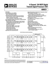
47. ANALOG 4 Channel 104 MSPS Digital DEVICES Transmit Signal Processor TSP AD6623 FEATURES Digital Resampling for Noninteger Interpolation Rates Pin Compatible to the AD6622 NCO Frequency Translation 18 Bit Parallel Digital IF Output Carrier Output from DC to 52 MHz Real or Interleaved Complex Spurious Performance Better than 100 dBc 18 Bit Bidirectional Parallel Digital IF Input Output Separate 3 Wire Serial Data Input for Each Channel Allows Cascade of Chips for Additional Channels Bidirectional Serial Clocks and Frames Clipped or Wrapped Over Range Microprocessor Control Two s Complement or Offset Binary Output 2 5 V CMOS Core 3 3 V Outputs 5 V Inputs Four Independent Digital Transmitters in Single Package JTAG Boundary Scan RAM Coefficient Filter RCF Programmable IF and Modulation for Each Channel Stati Programmable Interpolating RAM Coefficient Filter Mi 4 Pl C ilie pees 7 4 DOPSK Differential Phase Encoder FIDE base Stations 3 8 PSK Linear Encoder Wireless Local Loop Base Stations 8 PSK Linear Encoder Multicarrier Multimode Digital Transmit Programmable GMSK Look Up Table CMT 15136 PHS 1595 TDS CDMA UMTS Programmable QPSK Look Up Table All Pass Phase Equalizer Programmable Fine Scaler Programmable Power Ramp Unit High Speed CIC Interpolating Filter Phased Array Beam Forming Antennas Software Defined Radio Tuning Resolution Better than 0 025 Hz Real or Complex Outputs FUNCTIONAL BLOCK DIAGRAM
48. C2 is interpolating by a factor of five and the input signal has a bandwidth of 0 0033 of the CIC5 output sample rate Figure 32 shows 110 dBc rejection of the lower band edge of the first image All other image frequencies have better rejection Figure 32 Filtered rCIC2 Images Table XIV lists maximum bandwidth that will be rejected to various levels for CIC2 interpolation factors from 1 to 32 The example above corresponds to the listing in the 110 dB column and the L cic2 5 row The rejection of the CIC2 improves as the interpolation factor increases REV A AD6623 Table XIV Maximum Bandwidth of Rejection for Values 104 100dB 90dB 80dB 70 dB 1 Full Full Full Full Full 2 0 0023 0 0040 0 0072 0 0127 0 0226 3 0 0029 0 0052 0 0093 0 0165 0 0292 4 0 0032 0 0057 0 0101 0 0179 0 0316 5 0 0033 0 0059 0 0105 0 0186 0 0328 6 0 0034 0 0060 0 0107 0 0189 0 0334 7 0 0034 0 0061 0 0108 0 0192 0 0338 8 0 0035 0 0062 0 0109 0 0193 0 0341 9 0 0035 0 0062 0 0110 0 0194 0 0343 10 0 0035 0 0062 0 0110 0 0195 0 0344 11 0 0035 0 0062 0 0110 0 0195 0 0345 12 0 0035 0 0062 0 0111 0 0196 0 0346 13 0 0035 0 0062 0 0111 0 0196 0 0346 14 0 0035 0 0063 0 0111 0 0196 0 0346 15 0 0035 0 0063 0 0111 0 0197 0 0347 16 0 0035 0 0063 0 0111 0 0197 0 0347 17 0 0035 0 0063 0 0111 0 0197 0 0347 18 0 0035 0 0063 0 0111 0 0197 0 0348 19 0 0035 0 0063 0 0111 0 0197 0 0348 20 0 0035 0 0063 0
49. C2 provides fractional rate interpolation from 1 to 4096 in steps of 1 512 The wide range of interpolation factors in each CIC filter stage and a highly flexible resampler incorporated into rCIC2 makes the AD6623 useful for creating both narrowband and wideband carriers in a high speed sample stream The high resolution 32 bit NCO allows flexibility in frequency planning and supports both digital and analog air interface standards The high speed NCO tunes the interpolated complex signal from the rCIC2 to an IF channel The result may be real or complex Multicarrier phase synchronization pins and phase offset registers allow intelligent management of the relative phase of independent RF channels This capability supports the requirements for phased array antenna architectures and man agement of the wideband peak power ratio to minimize clipping at the DAC The wideband Output Ports can deliver real or complex data Complex words are interleaved into real I and imaginary Q parts at half the master clock rate AD6623 SPECIFICATIONS RECOMMENDED OPERATING CONDITIONS Test AD6623 Parameter Level Min Typ Max Unit VDD IV 2 25 2 5 2 75 V VDDIO IV 3 0 3 3 3 6 V Parameter Conditions Temp Test Level Min Typ Max Unit LOGIC INPUTS 5 V TOLERANT Logic Compatibility Full 3 3 V CMOS Logic 1 Voltage Full IV 2 0 5 0 V Logic 0 Voltage Full IV 0 3 0 8 V Logic 1 Current Full
50. CF modes and input data format that it sets Table I Serial Data Format Oxn0C Oxn0C Oxn0C Serial Data RCF Bit6 Bit 4 Word Length Mode 0 0 0 32 FIR 0 4 5 0 1 0 GMSK 0 1 1 MSK 1 0 0 24 Bit 9 is high FIR 16 Bit 9 is low compact 1 0 1 8 PSK 1 1 0 37 8 8 PSK 1 1 1 QPSK The serial data input SDIN accepts 32 bit words as channel input data The 32 bit word is interpreted as two 16 bit two s comple ment quadrature words I followed by Q MSB first This results in linear I and Q data being provided to the RCF The first bit is shifted into the serial port starting on the next rising edge of SCLK after the SDFO pulse Figure 16 shows a timing diagram for SCLK master SCS 0 and SDFO set for frame request SFE 0 CLK tsspio CLKn tosprooa isspio XXXXXXXXXXX XX Figure 16 Serial Port Switching Characteristics As an example of the Serial Port operation consider a CLK frequency of 62 208 MHz and a channel interpolation of 2560 In that case the input sample rate is 24 3 kSPS 62 208 MHz 2560 which is also the SDFO rate Substituting fsci 2 32 3 into the equation and solving for SCLKdivider we find the minimum value for SCLKdivider according to the equation below 32 3 Evaluating this equation for our example SCLKdivider must be less than or equal to 79 Since the SCLKdivider channel register is a 5 bit unsigned nu
51. E 22 0xn0D Channel Mode Control 2 40 FINE SCALE AND RAMP 22 xnOB Eie Scale Pact t cues saus EUR CAESA EE ew m ck 40 FINE SCALING kae orders tes 22 OxnOF RCF Time Slot Sync 40 RCF POWER RAMPING case ccs ase cme news DH Re 22 0 10 0 11 RCF Phase Equalizer Coefficients 40 Ramp Triggering a aka oa ees aches hou ers RE RI X CAE RUE 23 0xn12 0xn15 FIR PSK Magnitudes 40 Special Handling for SYNCO 23 0 10 Serial Port Setup eee OSG ae Rack 6 E 40 CASCADED INTERGRATOR COMB CIC 0xn17 Power Ramp Length 0 40 INTERPOLATING FILTERS 24 0xn18 Power Ramp Length 1 40 CIC Scaling vrss odes Por re core cR OR bare Rad CAI 24 0xn19 Power Ramp Rest Time 40 Tal cone sale a BUTI ace QURE Bue ac uma aen au basu 24 xn20 OxnlB Unused cesse n EE OO E OCA 40 The rCIC2 RESAMPLING INTERPOLATION FILTER 25 0xn20 0xn3F Data Memory 40 Permissible Values of L crc2 and 25 0xn40 0xn17F Power Ramp Coef
52. IC2 Decimation M 1 0x108 11 8 Reserved Ch A CCI2 Interpolation L 1 extended 7 0 Ch A C1C2 Interpolation L 1 No Change 0x109 7 0 Ch A C1C5 Interpolation L5 1 No Change 0x10A 15 8 Reserved Ch A RCF TapsB Nace 1 8 bits 7 Reserved Ch A TapsA Nacr 1 new MSB 6 0 Ch TapsA 1 7 bits No Change 0x10B 7 Reserved Ch A RCF Coef Offset new MSB 6 0 Ch A Coefficient Offset Ogcg 7 bits No Change 0x10C 15 10 Unused Reserved 9 Unused Ch A Compact FIR Input Word Length 0 16 bits 8 I followed by 8 Q 1 24 bits 12 I followed by 12 Q 8 Unused Ch A RCF PRBS Enable 7 Ch A PRBS Length Ch A RCF PRBS Length 0 15 0 15 1 8 388 607 1 8 388 607 6 Ch A RCF PRBS Enable Ch A RCF Mode Select 1 of 3 5 Ch Mode Select 1 of 2 Ch A RCF Mode Select 2 of 3 4 Ch A RCF Mode Select 2 of 2 Ch A RCF Mode Select 3 of 3 00 FIR 000 FIR 01 FIR 001 7 4 DQPSK 10 QPSK 010 GMSK 11 MSK 011 MSK 100 FIR Compact Input Resolution 101 8 PSK 110 31 8 8PSK 111 QPSK 3 0 Ch Taps per Phase 12 No Change 0x10D 7 6 Ch A RCF Coarse Scale a No Change 00 0 dB 01 6 dB 10 12 dB 11 18 dB 5 Ch A RCF Phase EQ Enable No Change 4 0 Ch A Serial Clock Divisor 2 4 64 Ch A Serial Clock Divisor 1 2 32 0 10 15 Ch A Serial Fine Scale Factor Enable Ch A Unsigned Scale Factor This is extended to allow values in the range 0 2 14 2 C
53. IV 1 10 uA Logic 0 Current Full IV 0 10 uA Input Capacitance 25 C V 4 pF LOGIC OUTPUTS Logic Compatibility Full 3 3 V CMOS TTL Logic 1 Voltage 0 25 mA Full IV 2 0 VDD 0 2 V Logic 0 Voltage 0 25 mA Full IV 0 2 0 4 V IDD SUPPLY CURRENT GSM Example CORE V 232 mA IO 56 mA IS 136 Example CORE V 207 mA IO 55 mA WBCDMA Example V TBD mA Sleep Mode Full IV TBD mA POWER DISSIPATION GSM Example V 740 mW IS 136 Example V 700 mW WBCDMA Example V TBD mW Sleep Mode Full IV TBD mW See the Thermal Management section of the data sheet for further details 4 REV A GENERAL TIMING CHARACTERISTICS AD6623 Test AD6623AS Parameter Conditions Temp Level Min Typ Max Unit CLK Timing Requirements Full I 9 6 ns tcrkr CLK Width Low Full IV 3 ns tcrkH CLK Width High Full IV 3 0 5 ns RESET Timing Requirement TRESL RESET Width Low Full I 30 0 ns Input Data Timing Requirements tsr INOUT 17 0 QIN to TCLK Setup Time Full IV 1 ns tur INOUTT 17 0 QIN to TCLK Hold Time Full IV 2 ns Output Data Timing Characteristics tpo TCLK to OUT 17 0 INOUT 17 0 QOUT Output Delay Time Full IV 2 6 ns tpzo OEN HIGH to OUTT 17 0 Active Full IV 3 7 5 ns SYNC Timing Requirements tss SYNC 0 1 2 3 to TCLK Setup Time Full IV 1 05 tus SYNC 0 1 2 3 to TCLK Hold Time Full IV 2 ns Master Mode Serial Port Timing Requirements SCS 0
54. Internal address notation read from left to right begins with Ox meaning the address that follows is hexadecimal The next three characters represent the address The first number or character is the MSB of the address If an n is present its value can be 1 2 3 or 4 and it depends upon the channel that is being addressed A B C or D The remaining two digits preceding the colon if present are the LSBs of the address If a colon follows the address then the succeeding digits tell the user what bit number s is are involved in decimal format For example 0xn24 7 0 SERIAL DATA PORT The AD6623 has four independent Serial Ports A B C and D and each accepts data to its own channel A B C or D of the device Each Serial Port has four pins SCLK Serial CLocK SDFO Serial Data Frame Out SDFI Serial Data Frame In and SDIN Serial Data INput SDFI and SDIN are inputs SDFO is an output and SCLK is either input or output depending the state of SCS Serial Clock Slave 0xn16 Bit 4 Each channel can be operated either as a Master or Slave channel depending upon SCS The Serial Port can be self framing or accept external framing from the SFDI pin or from the previous adjacent channel 0 16 Bits 7 and 6 Serial Master Mode SCS 0 In master mode SCLK is created by a programmable internal counter that divides CLK When the channel is sleeping SCLK is held low SCLK becomes active on the fir
55. MIGROPORT CONTROL 14 External Address 3 0 Data Bytes 36 OUTPUTS eet bre e RODA V Seam er ORA US 14 INTERNAL CONTROL REGISTERS AND ON CHIP RAM 36 JTAG AND BIST ei hdd nae sda X e E d 14 AD6623 and AD6622 Compatibility CONTROL REGISTER ADDRESS NOTATION 15 Common Function Registers not associated with a particular channel 36 SERIAL DATA PORT pde RR EXON 15 Channel Function Registers 0x1xx Ch A Serial Master Mode SCS 0 15 Ch B 0x3xx Ch C Ch D 36 Serial Slave Mode SCS lY AT RE xp RU 15 0x000 Summation Mode Control 38 Data Framing eee es pA RG eec KO 15 0x001 Sync Mode Control uu uke Pesce 44 ASR 38 Self Framing eee ay hee RARO ALS RA 15 0x002 BIST Counter z l usasqa ac des Rm e eed 38 External Framing Mode zu ere E ERE ode owe en RUE Ree 15 0x003 BIST Result usa MEE Rx ES ROUTE KOREAN ER Y 38 Serial Port Cascade Configuration 15 0xn00 Start Update Hold Off Counter 39 serial Data ce me en e DO ROME tel RE Poon 16
56. ND GND 103 VDD 104 SDFIA 105 TMS 106 TDI 108 TDO 107 SCLKA 109 VDDIO 110 SDFOA 111 SDINA 112 SCLKB 113 SDFOB 114 SDFIB 115 GND 116 SDFIC 117 SDINB 118 SCLKC 119 SDFOC 120 SDINC 121 VDDIO 122 SCLKD 123 SDFOD 124 SDIND 125 SDFID 126 VDD 127 GND 128 e I wli col si wielrellellej LO 2 ba Kas Gc Bs 0 cl ic SN est ES EEEE 9a aNd and 1noo 21110 9 110 LLno eLino LLLNO and OLLNO 61no 81no 4400 91no sino vino 1 1 Lino and aNd 11 REV A AD6623 128 LEAD FUNCTION DESCRIPTIONS Pin Number Mnemonic Type Description 1 3 5 9 19 21 31 32 34 36 38 39 GND P 42 52 54 64 65 68 72 83 85 95 96 98 99 102 103 116 128 2 OEN I Active High Output Enable Pin 29 28 27 25 24 23 22 18 17 16 15 OUT 17 0 O T Parallel Output Data 13 12 11 10 8 7 6 Ground Connection 47 59 66 104 127 VDD 2 5 V Supply 14 26 41 78 90 110 122 VDDIO P 3 3 V Supply 30 QOUT O T When HIGH indicates Q Output Data Complex Output Mode 33 37 40 43
57. R qe 24 Replaced Table XM i mdi pb ue S e WEA a ALERTE E VM ed e AAS a E US Lees Eb e Rd 25 Changes to Table Ba UAR Rar ble Rete Cede P PLNS See Te cane 25 Inserted new THE rCIC2 RESAMPLING INTERPOLATION FILTER section seeeeeee I e 25 R placed Equation 17 AWE eee ere HEY m eise e SU Ree eR enn ren E 25 Added Frequency Response of rCIC2 heading een hh hh 26 Added Programming Guidelines for AD6623 CIC Filters heading 1 ccc eee eee nent eee hern 26 Gh rnges to Table XIV Sarana tas UE M DER NR RE ei eee D ieu EVEN P EM EE 27 Changes to NUMERICALLY CONTROLLED OSCILLATOR TUNER section 27 Added Dual 18 Bit Output Configuration heading eee hh hahere a hr 28 Added Output Data Format heading uu L css fits as tees pm ih harka RD Ra Fel dex e Reime Ie E EU KH Qar haya 28 Added textto Output Data Format sectio ese ve un er RERO eR eer e oe dae LE Gr ME RT 28 Added O tput Clip Detection heading ua sua pu aaa RENE UP ROW dor uUi EQ PUN USANDO 28 Added Cascading Multiple AD6623s heading heh hh ra herren 28 Added Selection of Real and Complex Output Data Types heading ene ene nent ene hn 29 Added Hold Off Counter
58. RCF Coarse Scale dB 0 0 0 1 6 0 12 1 18 Bit 5 Bits 4 0 High enables the RCF phase equalizer Sets the serial clock divider SDIV that determines the serial clock frequency based on the following equation CLK Spry 1 0xn0E Fine Scale Factor 29 Bits 15 2 Sets the RCF Fine Scale Factor as an unsigned number representing the values 0 2 This register is shad owed for synchronization purposes The shadow can be read back directly the Fine Scale Factor can not Bits 1 0 Reserved 0xn0F RCF Time Slot Sync Bits 17 16 The Time Slot Sync Select bits are used to set which sync pin will initiate a time slot sync sequence The Fine Scale Hold Off Counter is used to syn chronize the change of RCF Fine Scale See the Synchronization section for a detailed explanation If no synchronization is required this register should be set to 0 0xn10 0xn11 RCF Phase Equalizer Coefficients See the RCF section for details 0xn12 0xn15 FIR PSK Magnitudes See the RCF section for details Bits 15 0 0xn16 Serial Port Setup Bits 7 6 Serial Data Frame Start Select Table XXV Serial Port Setup Bit 7 Bit 6 Serial Data Frame Start 0 X Internal Frame Request 1 0 External SDFI Pad 1 1 Previous Channels Frame End Bit 5 High means SDFO is a frame end low means SDFO is a frame request Bit 4 High selects serial slave mode SCLK is an input in serial slave mode
59. RCF filter Recalling the maximum equation from the RCF description are three restrictions to the RCF impulse response length Time Restriction CMEM Restriction amp mi 7 16x 236 32 4 DMEM Restriction where L X Lors X Loc _ Nrsp X 33 Jin De interleaving the input data into multiple TSPs extends the time restriction and may possibly extend the DMEM restriction but will not extend the CMEM restriction De interleaving the input stream to multiple TSPs divides the input sample rate to each TSP by the number of TSPs used Nysp To keep the output rate fixed L must be increased by a factor of which extends the time restriction This increase in L may be achieved by increasing any one or more of Lgcr Leics or Lcrc2 within their normal limits Achieving a larger L by increasing Lacy instead of Leics or Lcic2 will relieves the DMEM restriction as well In a UMTS example Nrsp 4 76 8 MHz and fn 3 84 MHz resulting in L 80 Factoring L into 10 Loic 8 and 1 results in a maximum 40 due to the time restriction Figure 42 shows an example RCF impulse response which has a frequency response as shown in Figure 43 REV A AD6623 RAM COEF FILTER DATA RE FORMATTER FILTER COMPLEX SIGNAL 32 BITS 16 I 16 Q 3 REAL OR IMAGINARY SIGNAL 9 6MSPS 9 6MSPS
60. RIPTION E ERE RE RM 3 Ser Prequency No Hop al u e mk pce Ra eon s 30 FUNCTIONAL OVERVIEW 3 Hop with SoftSyne usya a 30 RECOMMENDED OPERATING CONDITIONS 4 Pin Sync e pex ere ROC E E COE 30 ELECTRICAL CHARACTERISTICS 4 aaa eau qe edam deseen 31 LOGIC INPUTS 5 V TOLERANT 4 Set Phase No sw eR ad uqa 31 LOOIC OUTPUTS ii BERENS S Ee p Ed eR das 4 Beam with SoS Me was ye ek hh ex PKU EWE LEAR susu RR MESE EAE 31 IDD SUPPLY CURRENT ein x IU REX noe E ERREN EEA 4 Bini with Pin Syne vagiar or ee eines Fit ee rb ele n s 31 POWER DISSIPATION aa his Ree 4 Time Slot Ramp s uite taba rete eC FIA 31 GENERAL TIMING CHARACTERISTICS 5 Set Output Power No Ramp 31 MICROPROCESSOR PORT TIMING CHARACTERISTICS 6 Time Slot Ramp with SoftSync 31 MICROPROCESSOR PORT MODE INM MODE 0 6 Time Slot with Pin Syne ree E ewe bees 32 MICROPROCESSOR PORT MOTOROLA MODE 1 6 JTAG INTERFACE EX AREE Pee Mea 33 TIMING DIAGRAMS ik gas usakuy aa mi edere
61. The NCO Frequency contains a shadow register for synchronization purposes The NCO frequency can be read back directly however the shadow register cannot CLK NCO output frequency should not exceed approximately 45 of the CLK This makes allowance for the image filtering after D A conversion 0xn03 NCO Frequency Update Hold Off Counter See the Synchronization section for detailed explanation If no synchronization is required this register should be set to 0 Bits 17 16 The Hop Sync Select bits are used to set which sync pin will initiate a hop sequence Bits 15 0 The Hold Off Counter is used to synchronize the change of NCO frequencies 0xn04 NCO Phase Offset This register is 16 bit unsigned integer that is added to the phase accumulator of the NCO This allows phase synchronization of multiple channels of the AD6623 s The NCO Phase Offset contains a shadow register for synchronization purposes The shadow can be read back directly the NCO Phase Offset cannot See the Synchronization section for details 0xn05 NCO Phase Offset Update Hold Off Counter See the Synchronization section for a detailed explanation If no synchronization is required this register should be set to 0 Bits 17 16 The Phase Sync Select bits are used to set which sync pin will initiate a phase sync sequence gece 232 x JCHANNEL 27 Bits 15 0 The Hold Off Counter is used to synchronize the change of NCO phase
62. Y Figure 37 Block Diagram of Hardware and Software Sync Control for One AD6623 Sync Channel 32 REV A AD6623 JTAG INTERFACE The AD6623 supports a subset of IEEE Standard 1149 1 specifica tion For additional details of the standard please see IEEE Standard Test Access Port and Boundary Scan Architecture TEEE 1149 publication from IEEE The AD6623 has five pins associated with the JTAG interface These pins are used to access the on chip Test Access Port and are listed in Table XVII Table XVII Test Access Port Pins Name Pin Number Description TRST 100 Test Access Port Reset TCK 101 Test Clock TMS 106 Test Access Port Mode Select TDI 108 Test Data Input TDO 107 Test Data Output Note that TCK and TDI are internally pulled down which is opposite of IEEE Standard 1149 1 These pins may be connected to external pull up resistors with the associated additional current draw through the pull ups or left unconnected The AD6623 supports four op codes are shown in Table XVIII These instructions set the mode of the JTAG interface Table XVIII Op Codes Instruction Op Code IDCODE 10 BYPASS 11 SAMPLE PRELOAD 01 EXTEST 00 The Vendor Identification Code Table XIX can be accessed through the IDCODE instruction and has the following format Table XIX Vendor Identification Code phase offsets Nevertheless in most cases with a large number of carriers the worst case peak is an unlik
63. a the DAC used to produce an analog output signal will produce undesirable spectral components that should or must be suppressed Shaping or ramping the transition from no power to full power and vice versa reduces the amplitude of these spurious signals To program the ramp function a user must provide through the Microport the ramp memory RMEM coefficient values up to 64 number of RMEM coefficients to construct the ramp 1 to 64 and selection of a synchronizing signal source as discussed below The programmable power ramp up down unit allows power ramping on time slot basis as specified for some wireless transmission technologies e g TDMA The shape of the ramp is stored in RAM The RAM coefficients RMEM allow complete sample by sample control at the RCF interpolated rate This is particularly useful for time division multiplexed standards such as GSM EDGE A time slot or burst is ramped up and down by multiplying the Fine Scaled output of the RCF by a series of up to 64 ramp coefficients If more ramp resolution is required up to 64 interpolated coefficients can be added if the Ramp Interpolation bit 0xn16 1 is set to REV A AD6623 Logic 1 This extends the maximum ramp length to 128 coeffi cients Although the ramp is limited in length its time duration is a function of the output sample rate of the RCF multiplied by the ramp length Ramp duration is twice as long with Ramp Interpolation enabled tha
64. ability to synchronize channels or chips under microprocessor control One action to synchronize is the start of channels or chips The Start Update Hold Off Counter 0xn00 in conjunction with the Start bit and Sync bit Ext Address 5 allow this synchronization Basically the Start Update Hold Off Counter delays the Start of a channel s by its value number of AD6623 The following method is used to syn chronize the start of multiple channels via microprocessor control 1 Set the appropriate channels to sleep mode a hard reset to the AD6623 Reset pin brings all four channels up in Sleep Mode 2 Write the Start Update Hold Off Counter s 0xn00 to the appropriate value greater than 1 and less than 2181 If the chip s is not initialized all other registers should be loaded at this step 3 Write the Start bit and the Syncx s bit high Ext Address 5 4 This starts the Start Update Hold Off Counter counting down The counter is clocked with the AD6623 CLK signal When it reaches a count of one the sleep bit of the appropriate channel s is set low to activate the channel s Start with Pin Sync Four hardware sync pins are available on the AD6623 to pro vide the most accurate synchronization especially between multiple AD6623s Synchronization of start with an external signal is accomplished with the following method 1 Set the appropriate channels to sleep mode a hard reset to the AD6623 Reset pin brings all four chan
65. amp Length RO 1 0x118 4 0 Unused Ch A Mode 1 Ramp Length R1 1 0x119 4 0 Unused Ch A Ramp Rest Time Q No inputs requested during rest time Ox11A 11F Unused No Change 0x120 13F 15 0 Ch A Data RAM No Change 0x140 17F 15 14 Unused No Change 13 0 Unused Ch A Ramp RAM 0x180 1FF 15 0 Ch A Coefficient RAM No Change This address is mirrored at 0x900 0x97F and contiguously extended at 0x980 0x9FF NOTES Clear on RESET Allows dynamic updates 3These bits update after a Start or a Beam Sync See CR Ox10F 0x000 Summation Mode Control Controls features in the summation block of the AD6623 Bits 5 6 Reserved Bit 4 Low Wideband Input Enabled High Wideband Input Disabled Bit 3 Low Dual Output Disabled High Dual Output Enabled Bit 2 Reserved Bit 1 Low Output data will be in two s complement High Output data will be in offset binary Bit 0 Low Over range will wrap High Over range will clip to full scale 0x001 Sync Mode Control Bit 7 Ignores all but the first SyncO pulse Following this all 8 bits are cleared to completely mask off subse quent pulses Bit 6 Beam on pin Sync0 Bit 5 Bit 4 Bits 3 0 Hop on pin Sync0 High enables the count down of the Start Hold Off Counter The counter is clocked with the AD6623 CLK signal When it reaches a count of one the Sleep bit of the appropriate channel s is set low to activate the channel s High enables synchronization of these c
66. as a quadrature local oscillator running at fc x capable of producing any frequency step between fcix 2 and 2 with a resolution of 222 0 0242 Hz for 104 MHz The quadrature portion of the output is discarded Negative frequencies are distinguished from positive frequencies solely by spectral inversion The digital IF is calculated using the equation NCO frequency 232 fuco X where 22 NCO frequency is the decimal equivalent of the 32 bit binary value written to Oxn02 f r is the desired intermediate frequency in Hz and 18 forx 2 in Hz for complex outputs and fc in Hz for real outputs Phase Dither The AD6623 provides a phase dither option for improving the spurious performance of the NCO Phase dither is enabled by writing a 1 to Bit 3 of Channel Register 0xn01 When phase dither is enabled spurs due to phase truncation in the NCO are randomized The choice of whether phase dither is used in a system will ultimately be decided by the system goals and the choice of IF frequency The 18 most significant bits of the phase accumulator are used by the angle to Cartesian conversion If the NCO frequency has all zeroes below the 18 bit then phase dither has no effect If the fraction below the 18 bit is near 1 2 or 1 3 of the 189 bit then spurs will accumulate separated from the IF by 1 2 or 1 3 of the CLK frequency The smaller the denominator of this residual frac
67. ated carrier with linear ramp down and ramp up and rest time between ramps set to 30 RCF output sample time periods REV A Ramp Triggering The ramp sequence is triggered by the Fine Scale Hold Off counter The counter is loaded with a 16 bit user specified value 21 and lt 2 upon receipt of a sync pulse The counter then counts down master CLK cycles to 1 triggers the Ramp sequence and updates the Fine Scale factor The counter will then stop at a count of zero If the counter is initially loaded with 0 then the scale hold off counter is bypassed and will not trigger any succeeding events There are three ways to provide the sync pulse that loads the hold off counter that ultimately triggers the ramp 1 Serial Input sync This method is selected when Serial Time Slot Sync Enable 0xn16 2 is set to Logic 1 and appropriate serial word input bits are set as described in Figure 17 AD6623 Data Format and Bit Definition chart This allows a channel s Fine Scale Hold Off Counter to be loaded and a power ramp sequence to be triggered by a data word without resorting to hardware or software generated sync pulses This sync signal is routed to the OR gate following the Time Slot Sync multiplexer shown in the Sync Control block diagram Figure 37 2 Hardware Sync Sync Pins 0 1 2 and 3 provide a means to load the fine scale hold off counter using the channel s Time Slot Sync multiplexer The multiplexer allows selec
68. be generated Using the AD6623 to Process UMTS Carriers The AD6623 may be used to process two UMTS carriers each with an output oversampling rate of 24X i e 92 16 MSPS The AD6623 configuration used to accomplish this consists of using two processing channels in parallel to process each UMTS carrier Please refer to the Using the AD6623 to Process Two UMTS Carriers with 24X Oversampling section Digital to Analog Converter DAC Selection The selection of a high performance DAC depends on a number of factors The dynamic range of the DAC must be considered from a noise and spectral purity perspective The 14 bit AD9772A is the best choice for overall bandwidth noise and spectral purity In order to minimize the complexity of the analog interpolation filter which must follow the DAC the sample rate of the master clock is generally set to at least three times the maximum analog frequency of interest In the case where a 15 MHz band of interest is to be up converted to RF the lowest frequency might be 5 MHz and the upper band edge at 20 MHz offset from dc to afford the best image reject filter after the first digital IF The minimum sample rate would be set to 65 MSPS Consideration must also be given to data rate of the incoming data stream interpolation factors and the clock rate of the DSP Multiple TSP Operation Each of the four Transmit Signal Processors TSPs of the AD6623 can adequately reject the interpolation imag
69. cale should be increased by one In the preceding example if the worst case to channel center ratio is larger than 5 59 dB potentially overflowing the RCF and CIC then the Coarse Scale should be reduced by one and the Output Scale should be increased by one COEFFICIENT OdB TO 18dB MULTIPLIER RAMP MULTIPLIER SCALING WILL ATTENUATION RANGEISFROM RANGE 1 WITH AFFECT NUMER RANGE WITH 2WITH 16 BIT 14 RESOLUTION ICAL MAGNITUDE 2 BIT 6dB STEP RESOLUTION AND UP TO 128 SERIAL BASE DATA RESOLUTION RAMP DOWN STEPS BAND DATA IN 1 OF 4 CHANNELS RAM RCF FINE RCF POWER COEFFICIENT RUN SCALING RAMPING FILTER MULTIPLIER MULTIPLIER 18 BIT DIGITAL IF OUT CHANNEL NCO SUMMATION STAGE SCALING CIC CIC INTERPOLATION FILTERS SCALING 12dB TO 6dB 6dB TO 24dB 0dB TO 186 HARD WIRED ATTENUATION 6dB STEPS OUTPUT BIT RANGE WITH WITH 5 BIT SCALING IS 2 BIT 6dB STEP RESOLUTION AN OPTION RESOLUTION Figure 38 AD6623 Stage by Stage Summary of Available Scaling and Power Ramping Functions MICROPORT INTERFACE The Microport interface is the communications port between the AD6623 and the host controller There are two modes of bus operation Intel nonmultiplexed mode INM and Motorola nonmultiplexed mode MNM that is set by hard wiring the MODE pin to either ground or supply The mode is selected based on the use of the Microport control lines DS or RD DTACK or RDY RW or WR
70. d Time Full IV 8 0 ns tsAM Address Data RW WR Setup Time Full IV 3 0 ns THAM Address Data to RW WR Hold Time Full IV 2 0 ns tDDTACK DS RD to DTACK RDY Delay ns tacc RW WR to DTACK RDY Low Delay Full IV 4Xtcik 9XterK ns MODE MNM Read Timing tsc ControP to TCLK Setup Time Full IV 4 0 ns tuc Control to TCLK Hold Time Full IV 2 0 ns tups DS RD to DTACK RDY Hold Time Full IV 8 0 ns tsam Address to DS RD Setup Time Full IV 3 0 ns HAM Address to Data Hold Time Full IV 2 0 ns tzp Data Three State Delay Full IV ns tpp DTACK RDY to Data Delay Full IV ns DDTACK DS RD to DTACK RDY Delay Full IV ns tacc DS RD to DTACK RDY Low Delay Full IV 8Xtax 10 13x tck ns NOTES All Timing Specifications valid over VDD range of 2 375 V to 2 675 V and VDDIO range of 3 0 V to 3 6 V 2 oap 40 pF on all outputs unless otherwise specified 3Specification pertains to control signals RW WR DS RD CS Specifications subject to change without notice REV A AD6623 TIMING DIAGRAMS CLK RESET INOUT 17 0 OUT 17 0 QOUT inest OEN Figure 1 Parallel Output Switching Characteristics Figure 4 RESET Timing Requirements CLK toscLkH INOUT 17 0 SCLK QIN Figure 2 Wideband Input Timing Figure 5 SCLK Switching Characteristics Divide by 1 CLK CLK SCLK SYNC A Figure 3 SYNC Timing Inputs Figure 6 SCLK Switching Characterist
71. e No Change No Change No Change No Change No Change No Change No Change No Change No Change BIST Counter 2 BIST Value read only Channel Function Registers 0x1xx Ch A 0x2xx Ch B 0x3xx Ch C 0x4xx Ch D Internal Address Bit AD6622 Compatible Description AD6623 Extensions Description 0x100 17 16 Unused Ch A Start Sync Select 00 Sync0 See 0x001 01 Syncl 10 Sync2 11 Sync3 15 0 Ch A Start Hold Off Counter No Change 0x101 7 5 Reserved No Change 4 Ch A NCO Amplitude Dither Enable No Change 3 Ch A NCO Phase Dither Enable No Change 2 Ch A NCO Clear Phase Accumulator on Sync No Change 1 0 Ch A NCO Scale No Change 00 6 dB No Change 01 12 dB No Change 10 18 dB No Change 11 24 dB No Change 0x102 31 0 Ch A NCO Frequency Value No Change 0x103 17 16 Unused Ch A Hop Sync Select 00 Sync0 See 0x001 Hop 01 Syncl 10 Sync2 11 Sync3 15 0 Ch A NCO Frequency Update Hold Off Counter No Change 0x104 15 0 Ch A NCO Phase Offset No Change 36 REV AD6623 Channel Function Registers continued Internal Address Bit AD6622 Compatible Description AD6623 Extensions Description 0x105 17 16 Reserved Ch A Phase Sync Select 00 Sync0 See 0x001 Beam 01 Syncl 10 Sync2 11 Sync3 15 0 Ch A NCO Phase Offset Update Hold off Counter No Change 0x106 75 Reserved No Change 4 0 Ch A CIC Scale Scc No Change 0x107 8 0 Reserved Ch A C
72. e configured such that it begins processing 180 degrees out of phase with the primary channel The Start Holdoff Counter SHC of the secondary channel is set to the value of the primary channel plus LTOT 2 where L TOT is the overall channel interpolation Lror 34 2 For example in the case of LTOT 48 the primary channel of each processing is set to two while the secondary channel s Start Holdoff Counter is set to twenty six NCO Frequency Registers 0xn02 Bits 31 0 Each pair of processing channels must be assigned the same NCO Frequency Register values NCO Frequency Holdoff Counter 0xn03 Bits 15 0 Each pair of processing channels must be assigned the same NCO Holdoff Counter value NCO Phase Offset Register 0xn04 Bits 15 0 The NCO of the secondary channel must have its initial phase set such that when it begins processing its phase is equal to SCC chanel SCC channel REV A that of the primary channel s phase The equation is given by NCOPhaseOffset vnd fod Lo pd gt 35 J SAMP where round returns the nearest integer of its argument frac returns the fractional part of its argument is the desired NCO frequency and fsamr 15 the desire output sample rate NCO Phase Offset Update Holdoff 0xn05 Bits 15 0 Each pair of processing channels must be assigned the same NCO Phase Offset Update Holdoff value CIC Scale 0xn06 Bits 4 0 Each pair of processing channels must
73. e bit address bus A 2 0 Data Register 0 are needed Data Register 1 must be written first because write to Data Register triggers the internal access External Address 7 Upper Address Register UAR Data Register 0 must always be the last register written to initiate the Sets the four most significant bits of the internal address effectively internal write selecting channels 1 2 3 or 4 02 00 The autoincrement of read and write are also set 07 06 External Address 6 Lower Address Register LAR Sets the internal address 8 LSBs D7 D0 The Microport of the AD6623 allows for multiple accesses while Reading from the Microport is accomplished in a similar manner The internal address is first written A read from Data Register 0 activates the internal read thus Register 0 must always be read first to initiate an internal read This provides the 8 LSBs of the External Address 5 SoftSync internal read through the Microport D 7 0 Additional bytes This register is write only Bits in this address control the software are then read by changing the external address A 2 0 and synchronization or softsync of the AD6623 channels If the user performing additional reads If Data Register 3 or any other is intends to bring up channels with no synchronization requirements read before Data Register 0 incorrect data will be read Data or opts for Pin Sync control then all bits of this register should Register 0 mu
74. e final summation is then driven on the 18 bit Wideband Output Bus OUT 17 0 on the rising edge of the high speed clock If the OEN input is low then this output bus is three stated If the OEN input is high then this bus will be driven by the summed data The OEN is active high to allow the Wideband Output Bus to be connected to other busses without using extra logic Most other busses like 374 type registers require a low output enable which is opposite of the AD6623 OEN thus eliminating extra circuitry Dual 18 Bit Output Configuration The wideband parallel input IN 17 0 is defined as bidirectional to support dual parallel outputs Each parallel output produces the sum of two of the four internal TSPs and AD6623 that can drive two DACs Channels are added in pairs A B C D as shown in Figure 34 28 CHANNELS OUT A B 17 0 14 BIT DAC AD6623 14 BIT DAC CHANNELS IN OUT C D 17 0 Figure 34 AD6623 Driving Two DACs Output Data Format The Wideband Output Bus may be interpreted as a two s comple ment number or as an offset binary number as defined by Bit 1 of the Summation Mode Control Register at address 0x000 When this bit is high then the Wideband Output is in two s complement mode and when it is low it is configured for offset binary output data Offset binary data format is used when driving an offset binary DAC or test equipment etc that can accept offset binary The two s complement mode
75. e positive than the output can express and it will clip to 0x2000 for signals more negative than the output can express Cascading Multiple AD6623s The Wideband Input is always interpreted as an 18 bit two s complement number and is typically connected to the Wideband Output Bus of another AD6623 in order to send more than four carriers to a single DAC The Output Bus of the preceding AD6623 should be configured in two s complement mode and clip detection disabled The 18 bit resolution insures that the noise and spur performance of the wideband data stream does not become the limiting factor as large numbers of carriers are summed There is two clock cycle latency from the Wideband Input Bus to the Wideband Output Bus This latency may be calibrated out of the system by use of the Start Hold Off counter The preceding AD6623 in a cascaded chain can be started two CLK cycles before the following AD6623 is started and the data from each AD6623 will arrive at the DAC on the same clock cycle In systems where the individual signals are not correlated this is usually not necessary REV A AD6623 Selection of Real and Complex Output Data Types The AD6623 is capable of outputting both real and complex data When in Real mode the QIN input is tied low signaling that all inputs on the Wideband Input Bus are real and that all outputs on the Wideband Output Bus are real The Wideband Input Bus will be pulled low and no data will be added to
76. e resolution is approximately 10 ns and the delay range is from approximately 20 ns to 0 6 ms If a Hold Off Counter is loaded with 0 it will not respond to synchronizing pulses and the event will not be triggered by the hold off counter The AD6623 can trigger all of the aforementioned events except Ramping without a soft sync pin sync or data sync This is through the use of the Sleep bit for each channel at External Address 5 Whenever a channel is brought out of sleep mode sleep bit 4 low an automatic pulse updates all active and shadow registers This feature allows a channel to be reprogrammed while it is sleeping and then activated with immediate implementation of the changes Shadow Register are provided for three functions Frequency Hop Fine Scale and Phase Offset A shadow register precedes an active register It holds the next number to be used by the active register whenever that function s hold off counter causes the active register to be updated with the new value Active registers are also updated with the contents of a shadow register any time the channel is brought out of the sleep mode A shadow register is updated during normal programming of the registers through the Microport Active registers for frequency fine scale and phase offset words can only receive their update data from a shadow register When software reads back a channel s programmed values it is reading back the shadow registers of the fine
77. egin counting again The RCF Scale Hold off Counter counts master CLK cycles The REST time period is a programmable 5 bit value that counts interpolated RCF output samples before resuming serial input to the channel The succeeding actions of any hold off counter in the AD6623 can be defeat ed by setting its count value to 0 Figure 17 Data Formats Supported by the AD6623 when SCLK Master SCS 0 and SFDO Set for Frame Request SFE 0 REV A 17 AD6623 INTERPOLATING FIR PSK FILTER MODULATOR INTERPOLATING MSK MODULATOR INTERPOLATING QPSK DATA FROM SERIAL PORT MODULATOR Q ALLPASS PHASE EQUALIZER DATA TO CIC FILTERS Figure 18 RCF Block Diagram Table IV FIR Filter Internal Precision Minimum Maximum Signal x x y Notation Decimal Hexadecimal h Decimal Hexadecimal h I and Q Inputs 1 15 1 00000 1 00000 0 999969 0 FFFE Coefficients 1 15 1 00000 1 00000 0 999969 0 FFFE Product 2 18 0 99969 3 00020 1 000000 1 00000 Sum 4 18 7 00000 8 00000 7 999996 7 FFFFC FIR Output 1 17 1 00000 1 00000 0 999992 0 FFFF8 The Scale and Ramp block adjusts the final magnitude of the modulated RCF output synchronization pulse from the SYNCO 3 pins or serial words can be used to command this block to ramp down pause and ramp up to a new scale factor The shape of the ramp is stored in RAM allowing complete sample by sample control at the RCF interpolated rate This is particu
78. ely event The AD6623 immediately preceding the DAC can be programmed to clip rather than wrap around see the Summation Block description For a large number of carriers a rare but finite chance of clipping at the AD6623 wideband output will result in supe rior dynamic range compared to lowering each carrier level until clipping is impossible This will also be the case for most DACs Through analysis or experimentation an optimal output level of individual carriers can be determined for any particular DAC Single Carrier Scaling Once the optimal power level is determined for each carrier one must determine the best way to achieve that level The maximum SNR can be achieved by maximizing the intermediate power level at each processing stage This can be done by assuming the proper level at the output and working along the following path Summation NCO CIC Ramp RCF and finally Fine Scaler Unit The Summation Block is intended to combine multiple carriers with each carrier at least 6 dB below full scale For this configuration the AD6623 driving the DAC should have clip detection enabled OUT17 becomes a clip indicator that reports clipping in both polarities If the DAC requires offset binary outputs then the internal offset binary conversion should be enabled as well Any preceding cascaded AD6623s should disable clip detection and offset binary conversion The IN17 INO of the first AD6623 in the cascade should be grounded See the
79. ements azo XX VADADDRES lt top re n gt p VVV ora C mom RDY DTACK NOTES 1 tacc ACCESS TIME DEPENDS ON THE ADDRESS ACCESSED ACCESS TIME IS MEASURED FROM FE OF WR TO THE RE OF RDY 2 tacc REQUIRES A MAXIMUM OF 13 CLK PERIODS AND APPLIES TO 2 0 7 6 5 3 2 1 Figure 13 INM Microport Read Timing Requirements REV A TIMING DIAGRAMS MNM MICROPORT MODE CLK RW WR os XXN AAA AAA gt lt lsAM tham gt X gt tsam 3 vano vata kK RDY 5 1 tacc ACCESS TIME DEPENDS ADDRESS ACCESSED ACCESSTIME IS MEASURED FROM FE OF DS TOTHE FE OF DTACK 2 tacc REQUIRES A MAXIMUM 9 CLK PERIODS Figure 14 MNM Microport Write Timing Requirements tsc tups A 2 0 too gt tzp XXXXXXXXANX gt ipprack DTACK RDY ae NOTES 1 tacc ACCESS TIME DEPENDS ONTHE ADDRESS ACCESSED ACCESSTIME IS MEASURED FROM FE OF DS TOTHE FE OF DTACK 2 tacc REQUIRES A MAXIMUM 13 CLK PERIODS Figure 15 MNM Microport Read Timing Requirements AD6623 ABSOLUTE MAXIMUM RATINGS VDDIO A V eh ae apyu nie ce nae 0 3 V to 3 6 V VDD MEI 0 3 V to 2 75 V Input Voltage
80. equest Bit 5 0 Serial Clock Slave 0xn16 Bits 4 Each pair of processing channels must be configured in Master mode Bit 4 0 Performance The filter performance of the AD6623 s dual channel processing approach is shown in Figure 45 This filter uses 24 taps with RCF interpolation of 6 CIC5 interpolation of 8 and rCIC2 interpolation and decimation of 1 and 1 respectively The near rejection at 5 MHz is 65 dBc and rejection at 10 MHz is 80 dBc with a passband ripple of 0 25 dB The register settings implement ing this filter are outlined in the AD6623 Register Configuration section of this technical note 45 AD6623 CIC RESPONSE dBc COMPOSITE RESPONSE Figure 45 Composite Response to First CIC5 Null THERMAL MANAGEMENT The power dissipation of the AD6623 is primarily determined by three factors the clock rate the number of channels active and the distribution of interpolation rates The faster the clock rate the more power dissipated by the CMOS structures of the AD6623 and the more channels active the higher the overall power of the chip Low interpolation rates in the CIC stages CIC5 CIC2 results in higher power dissipation All these factors should be analyzed as each application has different thermal requirements The AD6623 128 Lead is specially designed to provide excellen
81. er A variety of processing options may be selected individually or in combination including PSK and MSK modulation FIR filtering all pass phase equalization and scaling with arbitrary ramping See Table III Table III Data Format Processing Options Processing Block Input Data Output Data Interpolating FIR Filter I and Q IandQ PSK Modulator 2 or 3 bits per symbol Unfiltered I and Q 4 5 8 PSK 3 8 8 8 MSK Modulator 1 bit per symbol Filtered MSK or GSM I and Q QPSK 2 bits per symbol Filtered QPSK IandQ All pass Phase Equalizer I and IandQ Scale and Ramp Iand Q IandQ REV A OVERVIEW OF THE RCF BLOCKS The Serial Port passes data to the RCF with the appropriate format and bit precision for each RCF configuration see Figure 17 The data may be modulated vectors or unmodulated bits I and Q vectors are sent directly to the Interpolating Fir Filter Unmodulated bits may be sent to the PSK Modulator the Interpolating MSK Modulator or the Interpolating QPSK Modulator The PSK Modulator produces unfiltered I and Q vectors at the symbol rate which are then passed through the Interpolating FIR Filter The Interpolating MSK Modulator and the Interpolating QPSK Modulator produce oversampled pulse shaped vectors directly without employing the Interpolating FIR Filter When possible the MSK and QPSK modulators are recommended for increased lt MSB I LSB gt AD6623 throughput and decrea
82. es of narrow band width carriers such as AMPS IS 136 GSM EDGE and PHS Wider bandwidth carriers such as 15 95 and IMT2000 require coordinated effort of multiple processing channels This section demonstrates how to coordinate multiple TSPs to create wider bandwidth channels without sacrificing image rejection As an example a UMTS carrier is modulated using four TSP channels an entire AD6623 The same principles can be applied to different designs using more or fewer TSPs This section does not explore techniques for using multiple TSPs to solve problems other than Serial Port or RCF throughput Designing filter coefficients and control settings for de interleaved TSPs is no harder than designing a filter for a single TSP For example if four TSPs are to be used simply divide the input data rate by four and generate the filter as normal For any design a better filter can always be realized by incrementing the number of TSPs to be used When it is time to program the TSPs only two small differences must be programmed First each channel is configured with exactly the same filter scalers modes and NCO frequency Since each channel receives data at one quarter the data rate and in a staggered fashion the Start Hold Off Counters must also be staggered see Programming Multiple TSPs section Second the phase offset of each NCO must be set to match the demultiplexed ratio in this example Thus the phase offset should be set
83. f the RCF is determined by the product of the number of interfering input samples Trcr and the RCF interpolation factor Lycr as shown by equation 8 below The values of Ngcr and Tgcr are programmed into control registers is not a control register but Ngcr and Trcr must be set so that is an integer If the integer interpolation by the RCF results in an inconvenient sample rate at the output of the RCF the desired output rate can usually be achieved by selecting non integer interpolation in the resampling CIC filter Nearer Tror X Lror 8 Trcr lt least is feo 19 AD6623 Table V Channel A RCF Control Registers Channel Bit Channel Bit Address Width Description Address Width Description 0 10 16 15 8 Nrcr 1 B 7 0 1 5 Ch A External SDFI Select Ox10B 8 7 0 0 Internal SDFI 0 10 10 9 Ch Compact FIR Input Word Length 1 External SDFI 0 16 bits 8 I followed by 8 Q 4 Ch A SCLK Slave Select 1 24 bits 12 I followed by 12 Q 0 Master 8 Ch A RCF PRBS Enable 1 Slave 7 Ch A RCF PRBS Length 3 Ch A Serial Fine Scale Enable 0 15 2 Ch A Serial Time Slot Sync Enable 1 8 388 607 ignored in FIR mode 6 4 Ch A RCF Mode Select 1 Ch A Ramp Interpolation Enable 000 FIR 0 Ch A Ramp Enable 001 7 4 DQPSK Modulator 0 117 6 5 0 Ch A Mode 0 Ramp Length RO 1 010 2 GMSK Look Up Table 0x118 6 5 0 Ch Mode 1 Ramp Length 1 1 011 MSK
84. ficient Memory 40 Frequency Response for CIC 26 Oxn80 OxnFF Coefficient Memory 40 Programming Guidelines for AD6623 CIC Filters 26 PSEUDOCODRE cay PE RR TE ee hades 40 NUMERICALLY CONTROLLED OSCILLATOR TUNER NCO 27 Write Pseudocode sie nsir reU RES E eee CES ame 40 Phase pus em ee oe Y I6 ome ye COINS w 27 Read Pseudocode gt e fot retard was ies 41 Amplitude Dither Vre eo ose drei 27 AD6623 EVALUATION PCB AND SOFTWARE 41 Phase Offset ashe cada ce acre rye 28 APPLICATIONS edle Edu 42 NCO Frequency Update and Phase Offset Using the AD6623 to Process UMTS Carriers 42 Update Hold Off Counters oo cux cure RR SE RE ES EN 28 Digital to Analog Converter DAC Selection 42 NOO Gontrol Seale haba qu xcd eed 28 Multiple TSP Operation s secer sa 42 SUMMATION BLOCK OS oae 28 Determining the Number of TSPs to Use 42 Dual 18 Bit Output Configuration 28 Programming Multiple TSPs 43 Output Data Format
85. gital signals to drive these TxDACs The RAM based architecture allows easy reconfiguration for multimode applications Modula tion pulse shaping and anti imaging filters static equalization and tuning functions are combined in a single cost effective device Digital IF signal processing provides repeatable manu facturing higher accuracy and more flexibility than comparable high dynamic range analog designs The AD6623 has four identical digital TSPs complete with synchronization circuitry and cascadable wideband channel summation AD6623 is pin compatible to AD6622 and can operate in AD6622 compatible control register mode The AD6623 utilizes a 3 3 V I O power supply and a 2 5 V core power supply All I O pins are 5 V tolerant All control registers and coefficient values are programmed through a generic micro processor interface Intel and Motorola microprocessor bus modes are supported All inputs and outputs are LVCMOS compatible FUNCTIONAL OVERVIEW Each TSP has five cascaded signal processing elements a programmable interpolating RAM Coefficient Filter RCF a programmable Scale and Power Ramp a programmable fifth order Cascaded Integrator Comb 5 interpolating filter a flexible second order Resampling Cascaded Integrator Comb filter rCIC2 and a Numerically Controlled Oscillator Tuner NCO The outputs of the four TSPs are summed and scaled on chip In multicarrier wideband transmitters a bidirectional bus all
86. h A RCF Unsigned Scale Factor No Change 1 0 Reserved Reserved 0 10 17 16 Unused Ch A Time Slot Sync Select 00 SyncO See 0x001 Beam 01 Syncl 10 Sync2 11 Sync3 15 0 Ch A RCF Scale Hold Off Counter The counter is unchanged but instead of just scale update when the counter hits one the following sequence is initiated 1 Ramp Down if Ramp is enabled 2 Update RCF Mode Select registers marked with 2 3 Ramp Up if Ramp is enabled REV A 37 AD6623 Channel Function Registers continued Internal Address Bit AD6622 Compatible Description AD6623 Extensions Description 0x110 15 0 Ch A RCF Phase EQ No Change 0 111 15 0 Ch A RCF Phase Coef2 No Change 0 112 15 0 Unused Ch A RCF FIR PSK Magnitude 0 0 113 15 0 Unused Ch A RCF FIR PSK Magnitude 1 Ox114 15 0 Unused Ch A RCF FIR PSK Magnitude 2 0 115 15 0 Unused Ch A RCF FIR PSK Magnitude 3 0 116 7 6 Unused Ch A Serial Data Frame Input Select Ox Internal Frame Request 10 External SDFI Pad 11 Previous Channel s Frame End 5 Unused Ch A Serial Data Frame Output Select 0 Serial Data Frame Request 1 Serial Data Frame End 4 Unused Ch A Serial Clock Slave SCS SCS 0 Master Mode SCLK is an output SCS 1 Slave Mode SCLK is an input 3 Unused Reserved 2 Unused Ch A Serial Time Slot Sync Enable ignored in FIR mode 1 Unused Ch A Ramp Interpolation Enable 0 Unused Ch A Ramp Enable 0 117 5 0 Unused Ch A Mode 0 R
87. hannels See the Synchronization section of the data sheet for detailed explanation 0x002 BIST Counter Sets the length in CLK cycles of the built in self test 0x003 BIST Result A read only register containing the result after a self test Must be compared to a known good result for a given setup to determine pass fail 38 REV A AD6623 0xn00 Start Update Hold Off Counter See the Synchronization section for detailed explanation If no synchronization is required this register should be set to 0 Bits 17 16 The Start Sync Select bits are used to set which sync pin will initiate a start sequence The Start Update Hold Off Counter is used to synchronize start up of AD6623 channels and can be used to synchronize multiple chips The Start Update Hold Off Counter is clocked by the AD6623 CLK master clock 0xn01 NCO Control Bit 1 0 Set the NCO scaling per Table XXII Table XXII NCO Control 0xn01 Bits 15 0 Bit1 Bit0 0 0 NCO Output Level 6 dB no attenuation 0 1 12 dB attenuation 1 0 18 dB attenuation 1 1 24 dB attenuation Bit 2 High clears the NCO phase accumulator to 0 on either a Soft Sync or Pin Sync see Synchronization for details High enables NCO phase dither High enables NCO amplitude dither Reserved and should be written low Bit 3 Bit 4 Bits 7 5 0xn02 NCO Frequency This register is a 32 bit unsigned integer that sets the NCO Frequency
88. hardware pin sync signal SYNCI 2 and 3 are directly routed to the multiplexer whereas SYNCO is routed through two AND gates before it reaches the multiplexer The AND gates duplicate the AD6622 single sync pin function to allow pin compatibility SYNCO is routed in parallel to both the Beam and Time Slot multiplexers and it is a shared signal after is has been enabled at 0x001 6 0x001 4 START SYNC To use SYNCI 2 or 3 simply set the select lines according to the Channel Register address 0xn0F 16 17 for the desired sync signal Attach a sync signal source to the package pin When it is time to sync assert a Logic high minimum 1 CLK period 2 ns duration and return to Logic 0 This loads the Fine Scale Hold Off Counter and a countdown commences Holding a logic high at the chosen sync input pin longer than needed will result in additional delay as the Scale Hold Off Counter is continually loaded with the same beginning count From the Block Diagram Figure 37 it can be seen note the OR gates at the output of each multiplexer that a software sync can also be used in conjunction with a hardware sync without any modification to the hardware setup SYNCO is selected at the Time Slot multiplexer using the same select lines at OxnOF 16 17 as for SYNC 1 2 and 3 however two additional masking registers must be dealt with to get SYNCO routed to the Time Slot Sync multiplexer First SYNCO mu
89. hieved with the AD6623 These are Start Hop and Beam Each is described in detail below The synchronization is accomplished with the use of a shadow register and a Hold Off counter See Figure 36 for a simplistic schematic of the NCO shadow register and NCO Frequency Hold Off counter to understand basic operation Enabling the clock AD6623 CLK for the Hold Off counter can occur with either a Soft Sync via the Microport or a Pin Sync The functions that include shadow registers to allow synchronization include l Start 2 Hop NCO Frequency 3 Beam NCO Phase Offset Hold Off Counters and Shadow Registers Hold Off Counters are used with the five synchronized AD6623 functions e Start of Channel s RCF Fine Scale output level update Power Ramping of Time Slot transmissions e Frequency Hopping e Phase Shifting for Beam ControlStart REV A These are 16 bit counters that are preloaded with a programmable value upon receipt of a synchronizing pulse The counter then counts down to zero and stops The counters are re triggerable during countdown If the counter is re triggered it re loads its count value and starts again and may preclude the triggering of the event as intended When the count reaches one a trigger signal is emitted which causes the desired event Start Ramp Hop Beam Scale to commence The counters are clocked with the AD6623 CLK that determines the time resolution of the each count With 104 MHz th
90. ic Divide by 2 or EVEN Integer CLK SCLK Figure 7 SCLK Switching Characteristic Divide by 3 or ODD Integer REV A 7 AD6623 SCLK SDFO Figure 8 Serial Port Timing Master Mode 5 5 0 Channel is Self Framing SDFO DH tsspn tus X _ Figure 9 Serial Port Timing Slave Mode SCS 1 Channel is Self Framing nCLKs tpsrooB SDFO tssrio tusrio SDFI toe gt EE pgo som _ Figure 10 Serial Port Timing Master Mode SCS 0 Channel is External Framing nCLKs SCLK gt 1 SDFO tssFn lt SDFI Coe lt lt tuson _ _ 99 Figure 11 Serial Port Timing Slave Mode SCS 1 Channel is External Framing 8 REV A AD6623 TIMING DIAGRAMS INM MICROPORT MODE es XXN XXX AAA toa tHam e iau 47 OU XA vano para ion RDY DTACK tacc NOTES 1 tacc ACCESS TIME DEPENDS ONTHE ADDRESS ACCESSED ACCESSTIME IS MEASURED FROM FE OF WR TOTHE RE OF RDY 2 tacc REQUIRES A MAXIMUM 9 CLK PERIODS Figure 12 INM Microport Write Timing Requir
91. inually adjust the period by one SCLK cycle to keep the average SDFO rate equal to the input sample rate When the channel is in sleep mode SDFO is held low The first SDFO is delayed by the channel reset latency after the Channel Reset is removed The channel reset latency varies dependent on channel configuration External Framing Mode In this mode Bit 7 of register 0xn16 is set high The external framing can come from either the SDFI pin 0xn16 Bit 6 0 or the previous adjacent channel 0xn16 Bit 6 1 In the case of external framing from a previous channel it uses the internal frame end signal for serial data frame synchronizing When in master mode SDFO and SDFI transition on the positive edge of SCLK and SDIN is captured on the positive edge of SCLK When in slave mode SDFO and SDFI transition on the negative edge of SCLK and SDIN is captured on the negative edge of SCLK Serial Port Cascade Configuration In this case the SDFO signal from the last channel of the first chip would be programmed to be a serial data frame end SFE 0xn16 Bit 5 1 This SDFO signal would then be fed as an input for the second cascaded chip s SDFI pin input The second chip would be programmed to accept external framing from the SDFI pin 0xn16 Bit 7 1 Bit 6 0 15 AD6623 Serial Data Format The format of data applied to the serial port is determined by the RCF mode selected in Control Register OxnOC Below is a table showing the R
92. ister allows multiple NCOs to be synchronized to produce sine waves with a known phase relationship NCO Frequency Update and Phase Offset Update Hold Off Counters update of both the NCO frequency and phase offset can be synchronized with internal Hold Off counters Both of these counters are 16 bit unsigned integers and are clocked at the master CLK rate These Hold Off counters used in conjunction with the fre quency or phase offset registers allow beam forming and frequency hopping See the Synchronization section of the data sheet for additional details The NCO phase can also be cleared on Sync set to 0x0000 by setting Bit 2 of Channel Register 0xn01 high NCO Control Scale The output of the NCO can be scaled in four steps of 6 dB each via Channel Register Oxn01 Bits 1 0 Table XV show a breakdown of the NCO Control Scale The NCO always has loss to accommodate the possibility that both the I and Q inputs may reach full scale simultaneously resulting in a 3 dB input magnitude Table XV NCO Control Scale 0 01 Bit 1 0xn01 Bit 0 NCO Output Level 0 0 6 dB no attenuation 0 1 12 dB attenuation 1 0 18 dB attenuation 1 1 24 dB attenuation SUMMATION BLOCK The Summation Block of the AD6623 serves to combine the outputs of each channel to create a composite multicarrier signal The four channels are summed together and the result is then added with the 18 bit Wideband Input Bus IN 17 0 Th
93. larly useful for time division multiplexed standards such as GSM EDGE Modulator configurations can be updated while the ramp is quiet allowing for GSM and EDGE timeslots to be multiplexed together without resetting or reconfiguring the channel Each of the RCF processing blocks is discussed in greater detail in the following sections INTERPOLATING FIR FILTER The Interpolating FIR Filter realizes a real sum of products filter on I and Q inputs using a single interleaved Multiply Accumulator MAC running at the CLK rate The input signal is interpolated by integer factors to produce arbitrary impulse responses up to 256 output samples long Each bus in the data path carries bipolar two s complement values For the purpose of discussion we will arbitrarily consider the radix point positioned so that the input data ranges from 1 to just below 1 In Figure 19 the data buses are marked x x y to denote finite precision limitations A bus marked x x y has x bits above the radix and y bits below the radix which implies a range from 2 to 2 1 27 in 2 steps The range limits are tabulated in Table IV for each bus The hexadecimal values are bit exact and each MSB has negative weight Note that the Product bus range is limited by result of the multiplication and the two most significant bits are the same except in one case 18 20 271 272 OR 2 3 Figure 19 Interpolating FIR Filter Block Diagram The RCF realizes a FIR filter
94. low must be set HIGH whenever RMEM ramp memory CMEM coefficient memory or DMEM data memory are to be programmed However when programming is completed the PROG bit for the channel s must be returned LOW for proper channel functioning Set Output Power No Ramp The steps below assume that the user has established a data flow from input to output of the AD6623 1 Place the channel s in SLEEP Mode external address 4 3 0 write bit s high 2 Set bit 0 of Internal Address 0xn16 the channel s Ramp Enable bit to Logic 0 This defeats the ramp function 3 Set the fine scaling and coarse scaling control register values associated with the RCF 0xn0D 7 6 and 0 0 15 2 CIC 0xn06 4 0 NCO 0xn01 1 0 and SUMMATION stages to the desired levels according to the SCALING section of this data sheet 4 Finally re establish an output data flow to a DAC by bringing the appropriate SLEEP bits low and verify desired signal ampli tude Note a START sync pulse is automatically generated when the channel is brought out of SLEEP Mode The START pulse loads the updated control register data to the appropriate active counters and shadow registers Time Slot Ramp with SoftSync Time Slot or ramping functions for each channel can be engaged with software synchronizing words received through the Micro port The RCF Fine Scale Hold Off Counter in conjunction with the Beam bit which is the sync signal and SyncA B C and or D
95. m REV 0 to REV A Changes FEATURES ayy ai ee ert RR ONE ER E IRURE ap duis Ra PCR NS baat CERCHI OUR T c canton Og tented ORC RES 1 Ghang sto TABLE OF CONTENTS Ca z crap Re epe wei ide Im e desk ES Ou de ku red ere T 2 Changes to RECOMMENDED OPERATING CONDITIONS s essel hh he heh hh 4 Changes to ELECTRICAL CHARACTERISTICS a sss s aun hh heh he me hh hes 4 Ghanges to THERMAL CHARACTERISTICS iude due ep E Rae REX P Ies VK PR E E IER MU 10 Changes to ORDERING GUIDE et e motn PA E S ce SUR ARR Ge prt cited e gi bro eite Ros eod E Rd DR E E SURE 10 Added CONTROL REGISTER ADDRESS NOTATION section Rh hr rr hen 15 Added Serial Data Eraming section seed desk doe eot edes Force kaya e arl e estab Ee kanasta Yana NS ete crar sles eR a 15 Editsto Tablel ue Leh eds Saw PE URBAN EU NE Ae Gee QUE Mae US EI RI ER 16 Edits to Table IE z cereales Eu eese e taie eei d T ed es 16 Added Notes and Legend to Figure 17 ia operie one dae eet ga ett nU AIRES OUR P Cut tates due HERRERA EX eH des ates 17 Changes to INTERPOLATING FIR FILTER section 2 0 0 eee hh hahahaha hrs 18 Renamed and Changed Table V us ce eerie nu gre tern aca Saya sqa Za eu e dx ger We a apaqay lang doe e coc 20 Changes to 7 4 DQPSK Modulation section
96. mber it can only range from 0 to 31 Any value in that range will be valid for this example but if it is important that the SDFO period is constant then there is another restric tion For regular frames the ratio amp must be equal to an integer of 22 or larger For this example constant SDFO periods can only be achieved with an SCLK divider of 31 or less SCLKdivider 16 See Table II for usable SCLK divider values and the corre sponding SCLK and fscrxffspro ratio for the example of L 2560 In conclusion SDFO rate is determined by the AD6623 CLK rate and the interpolation rate of the channel The SDFO rate is equal to the channel input rate The channel interpolation is equal interpolation times CIC5 interpolation times CIC2 interpolation L L Lacy X Leics X eem 4 Monica The SCLK divide ratio is determined SCLKdivider as shown in equation 3 The SCLK must be fast enough to input 22 bits of data prior to the next SDFO Extra SCLKs are ignored by the serial port Table II Example of Usable SCLK Divider Values and fsciy fspgo Ratios for L 2560 SCLKdivider fscuxl fspro 0 2560 1 1280 3 640 4 512 7 320 9 256 15 160 19 128 31 80 PROGRAMMABLE RAM COEFFICIENT FILTER RCF Each channel has a fully independent RAM Coefficient Filter The RCF accepts data from the Serial Port processes it and passes the resultant I and Q data to the CIC filt
97. n when it is not enabled The channel s Ramp Enable bit at control register address 0 16 bit 0 must be set to Logic 1 or else the ramp function will be bypassed and the RCF output data is passed unaltered to the CIC interpolation stages When in use the maximum signal gain is dependent on what value is stored in the last valid RMEM ramp memory location RMEM words are 14 bits with a range of 0 1 When the ramp is triggered the following sequence occurs see Figures 26 and 27 RAMP DOWN beginning at the last coefficient of the specified ramp length and proceeding sample by sample to the first coefficient Next a REST or quiet period from 0 to 32 RCF output samples duration occurs During this time the Mode bit as shown in Figure 17 AD6623 Data Format and Bit Definition chart is updated input sampling is halted and any control register with a superscript 2 is updated Modulator configurations can be updated while the ramp is quiet allowing for GSM and EDGE timeslots to be multiplexed without resetting or reconfiguring the channel Lastly RAMP UP occurs beginning at the first coefficient and ending at the last coefficient of the specified length The final output level from the ramp stage is equal to the RCF Fine Scale output level multiplied by the last ramp coefficient Figure 26 View of an unmodulated carrier with linear ramp down and ramp up and rest time between ramps set to 0 Figure 27 View of an unmodul
98. nal Address 7 allow the user to set the address to auto increment after reads writes or both All internal data words have widths that are less than or equal to 32 bits Accesses to External Address 0 also triggers access to the AD6623 s internal memory map Thus during writes to the Internal Registers External Address 0 must be written last to insure all data is transferred Reads are the opposite in that External Address 0 must be the first data register read after setting the appropriate internal address to initiate an internal access External Address 5 4 reads and writes are transferred immediately to Internal Control Registers External Address 4 is the sleep register The sleep bits can be set collectively by the address The sleep bits can be cleared by operation of start syncs as shown in Table XXI REV A AD6623 Table XXI External Registers External Data External Address D7 D6 D5 D4 D3 D2 D1 DO 7 Wrinc Rdinc IAII IAIO IA9 IA8 6 LAR IA7 IA6 IA5 4 2 IA1 TAO 5 SoftSync Beam Hop Start Sync D Sync C Sync B Sync A 4 Sleep Prog D Prog C Prog B Prog A Sleep D Sleep C Sleep B Sleep A 3 Byte3 ID31 ID30 ID29 ID28 ID27 ID26 ID25 ID24 2 Byte2 ID23 ID22 ID21 ID20 ID19 ID18 ID17 ID16 1 Bytel 1015 1014 ID13 ID12 010 109 108 0 ByteO ID7 ID6 ID5 ID4 ID3 ID2 IDI IDO External Address 5 is the Sync register These bits are write Intel Nonmultiplexed Mode INM
99. nels up in sleep mode 2 Write the Start Update Hold Off Counter s 0xn00 to the appropriate value greater than 1 and less than 2 1 If the chip s is not initialized all other registers should be loaded at this step 30 3 Set the Start on Pin Sync bit and appropriate Sync Pin Enable high 0xn01 4 When the Sync pin is sampled high by the AD6623 CLK this enables the count down of the Start Update Hold Off Counter The counter is clocked with the AD6623 CLK signal When it reaches a count of one the sleep bit of the appropriate channel s is set low to activate the channel s Hop A jump from NCO frequency to new NCO frequency This change in frequency can be synchronized via microprocessor control or an external Sync signal as described below To set the NCO frequency without synchronization the following method should be used Set Frequency No Hop 1 Set the NCO Frequency Hold Off Counter to 0 2 Load the appropriate NCO frequency The new frequency will be immediately loaded to the NCO Hop with SoftSync The AD6623 includes the ability to synchronize a change in NCO frequency of multiple channels or chips under microprocessor control The NCO Frequency Hold Off Counter 0xn03 in conjunction with the Hop bit and the Sync bit Ext Address 5 allow this synchronization Basically the NCO Frequency Hold Off counter delays the new frequency from being loaded into the NCO by its value number of AD6
100. nter value L Nrsp larger than its predecessor s If the TSPs are located on cascaded AD6623s the Hold Off Counters of the upstream device should be incremented by an additional one In the UMTS example L 80 and Nrsp 4 so to respond as quickly as possible to a Start SYNC the Hold Off Counter values should be 1 21 41 and 61 REV A Driving Multiple TSP Serial Ports When configured properly the AD6623 will drive each SDFO out of phase Each new piece of data should be driven only into the TSP that pulses its SDFO pin at that time In the UMTS example in Figure 41 L 80 and Nrsp 4 so each serial port need only accept every fourth input sample Each serial port is shifting at peak capacity so sample 1 2 and 3 begin shifting into Serial Ports B C and D before sample 0 is com pleted into Serial Port A SDFOA SDFOB n n SDFOC m n l SDFOD Ue s Figure 41 UMTS Example 1 0 0 5 MAGNITUDE 0 0 0 5 10 15 20 25 30 35 40 COEFFICIENT Figure 42 Typical Impulse Response for WBCDMA Wide Band Code Division Multiple Access 43 9 16 02 12 30 PM TG AD6623 dBc 0 1000 2000 3000 4000 5000 6000 7000 8000 9000 10000 kHz Figure 43 RAM Coefficient Filter Frequency Response for WBCDMA dBc COMPOSITE AD6623 RESPONSE IDEAL FILTER MIT MTM
101. of Sync0 a hardware sync pulse for Time Slot Sync may require bits in several registers to be set depending upon the number of active channels These control bits are located in the Internal Common Function Registers address 0x001 and the Internal Channel Function Registers address 0 00 0xn03 0xn05 OxnOF Address 0x001 contains 8 bits that will mask the distribution of pin sync pulses from Sync0 to all channels and enable which sync multiplexers start hop and beam receive SyncO pulses Furthermore the MSB at 0x001 is a First Sync Only flag that when high allows only one SyncO pulse to be routed to the selected sync block s Following this all 8 bits of register 0x001 are cleared to completely mask off subsequent pulses 23 AD6623 Sync pulses from Syncl 2 and 3 pins are not masked in any fash ion and directly connect to all Sync multiplexers of all channels The Sync Control Block Diagram Figure 37 in the Synchronization section of this data sheet provides an overview of all sync signal routing for one channel CASCADED INTEGRATOR COMB CIC INTERPOLATING FILTERS The I and Q outputs of the RCF stage are interpolated by two cascaded integrator comb CIC filters The CIC section is separated into three discrete blocks a fifth order filter CIC5 a second order resampling filter rCIC2 and a scaling block CIC Scaling The CIC5 and rCIC2 blocks each exhibit a gain that changes with respect to thei
102. only There are three types of Syncs Start Hop and Beam Each MODE must be tied low to operate the AD6623 Microport in of these can be sent to any or all of the four channels For example INM mode The access type is controlled by the user with the a write of X0010100 would issue a start sync to Channel C only chip select CS read RD and write WR inputs The ready A write of X1101111 would issue a Beam Sync and a Hop Sync to RDY signal is produced by the Microport to communicate to all channels the user the Microport is ready for an access RDY goes low at The internal address bus is 12 bits wide and the internal data bus the start of the access and is released when the internal cycle is is 32 bits wide External address 7 is the UAR Upper Address complete See the timing diagrams for both the read and write Register and stores the upper four bits of the address space in modes in the Specifications UAR 3 0 UAR 7 6 define the auto increment feature If Bit 6 Motorola Nonmultiplexed Mode MNM is high the internal address is incremented after an internal read MODE must be tied high to operate the AD6623 Microport in If Bit 7 is high the internal address is incremented after an internal MNM mode The access type is controlled by the user with the write If both bits are high the internal address in incremented chip select CS data strobe DS and read write RW inputs after either a write or a read This feature is designed for seq
103. ows the Parallel wideband IF Input Output to drive a second DAC In this operational mode two AD6623 channels drive one DAC and the other two AD6623 channels drive a second DAC Multiple AD6623s may be combined by driving the INOUT 17 0 of the succeeding with the OUTT 17 0 of the preceding chip The REV A INOUTT 17 0 can alternatively be masked off by software to allow preceding AD6623 s outputs to be ignored Each channel accepts input data from independent serial ports that may be connected directly to the serial port of Digital Sig nal Processor DSP chips The RCF implements any one of the following functions Inter polating Finite Impulse Response FIR filter 7 4 DQPSK modulator 8 PSK modulator or 3 8 8 8 modulator GMSK modulator and QPSK modulator Each AD6623 channel can be dynamically switched between the GMSK modulation mode and the 31 8 8 5 modulation mode in order to support the GSM EDGE standard The RCF also implements an Allpass Phase Equalizer APE which meets the requirements of 15 95 standard CDMA transmission The programmable Scale and Power Ramp block allows power ramping on a time slot basis as specified for some air interface standards e g GSM EDGE A fine scaling unit at the pro grammable FIR filter output allows an easy signal amplitude level adjustment on time slot basis The CIC5 provides integer rate interpolation from 1 to 32 and coarse anti image filtering The rCI
104. plex Output Mode off 0 on 1 ceil when a value within the parenthesis is not an integer then round up to the next integer e g 9 001 10 Leics Interpolation rate of CIC5 L cic2 Interpolation of rCIC2 Decimation of rCIC2 25 AD6623 Resampling is implemented by apparently increasing the input sample rate by the factor L using zero stuffing for the new data samples Following the resampler is a second order cascaded integrator comb filter Filter characteristics are determined only by the fractional rate change L M The filter can produce output signals at the full CLK rate of the AD6623 The output rate of this stage is given by the equation below L Sour 101 2 19 Merce Both L cic2 and are unsigned integers The interpolation rate L cic may be from 1 to 4096 and the decimation M crc2 may be between 1 and 512 The stage can be bypassed by setting the L and M to 1 The transfer function of the rCIC2 is given by the following equations with respect to the rCIC2 output sample rate four 1 z Lee rCIC2 z EE 20 Frequency Response of rCIC2 The frequency response of the rCIC2 can be expressed as follows The maximum gain is L crc2 at baseband The initial M circ2 L crc2 factor normalizes for the increased rate which is appropriate when the samples are destined for a DAC with a zero order hold output 2 sin s ERA i M rCIC2 f 192 iae L cc2
105. r rate change factors Licico and Lcrcs The product of these gains must be compensated for in a shared CIC Scaling block and can be done to within 6 dB The remaining compensation can come from the RCF in the form of coefficient scaling or the fine scaling unit CIC Scaling The scale factor is a programmable unsigned integer between 4 and 32 This is a combined scaler for the CIC5 and rCIC2 stages The overall gain of the CIC section is given by the equation below CIC Gain Loes X Lc X 25 10 CICS The first CIC filter stage the CICS is fifth order interpolating cascaded integrator comb whose impulse response is completely defined by its interpolation factor Lcrcs The value Lcrcs 1 be independently programmed for each channel at location 0xn09 j Lcics CIC SCALE CIC5 rcic2 Figure 28 CIC5 While this control register is 8 bits wide should be confined to the range from 1 to 32 to avoid the possibility of internal overflow for full scale inputs The output rate of this stage is given by the equation below X Lcics 11 The transfer function of the CIC5 is given by the following equations with respect to the CIC5 output sample rate fgayps 2 SCIC 4 1 g 2 12 The SCIC value can be independently programmed for each channel at Control Register 0xn06 Scrc may be safely calculated according to equation 13 below to
106. rier scaling and single carrier scaling Multicarrier Scaling An arbitrary number of AD6623s can be cascaded to create composite digital IF with many carriers As the number of carriers increases the peak to rms ratio of the composite digital IF will increase as well It is possible and beneficial to limit the peak to rms ratio through careful frequency planning and controlled REV A The NCO Tuner is equipped with an output scaler that ranges from 6 02 dB to 24 08 dB below full scale in 6 02 dB steps See the NCO Tuner section for details The best SNR will be achieved by maximizing the input level to the NCO and using the largest possible NCO attenuation For example to achieve an output level 20 dB below full scale one should set the CIC output level to 1 94 dB below full scale and attenuate by 18 06 dB in the NCO The CIC is equipped with an output scaler that ranges from 0 dB to 186 64 dB below full scale in 6 02 dB steps This large attenuation is necessary to compensate for the potentially large gains associated with CIC interpolation See the CIC section for details For example to achieve an output level of 1 94 dB below full scale with a CIC5 interpolation of 27 114 51 dB gain and CIC2 interpolation of 3 9 54 dB gain one should set the CIC Scale to 20 and the Fine Scale Unit output level to 5 59 dB below full scale 33 AD6623 1 94 9 54 114 514 20 x 6 02 5 59 23
107. rresponding coefficient weight from positive full scale through zero to negative full scale is illustrated in Table X 22 Table X Coefficient Weights Register Value Coefficient Weight Ox7FFF 1 999938964844 0x0001 0 00006103515625 0x0000 0 OxFFFF 0 00006103515625 0 8001 1 999938964844 0 8000 2 Table XI shows the recommended b and coefficients for the respective oversampling rate Table XI b and b Coefficients Over sampling b b b 1 1 0 25421 0 efbbh 0 11188 0 0729h 2 1 0 96075 0 c283h 0 33447 0 1568h 3 1 1 28210 0 adf2h 0 48181 0 1ed6h 4 1 1 45514 0 a2dfh 0 57831 0 2503h 5 1 1 56195 0 9c09h 0 64526 0 294ch 6 1 1 63409 0 976bh 0 69415 0 2c6dh 7 1 1 68604 0 9418h 0 73132 0 2eceh 8 1 1 72516 0 9197h 0 76050 0 30ach FINE SCALE AND POWER RAMP Fine Scale multiplier factors in the range 0 2 with a step resolution of 2 19 Power Ramp multiplier factors in the range 0 1 with a step resolution of 2 14 FINE SCALING Fine Scale multiplier factors range from 0 2 with a step resolution of 2 in the AD6622 emulation mode and 218 in AD6623 emulation mode Scaling values for each channel are pro grammed at register OxnOE in the AD6623 internal memory using the Microport interface RCF POWER RAMPING When the output of the AD6623 is programmed to be a rapid series of on off bursts of dat
108. s REV A 0xn06 CIC Scale Bits 4 0 Sets the CIC scaling per the equation below CIC Scale ceil x loz Lo apana 28 See the CIC section for details 0xn07 CIC2 Decimation 1 Mcic gt 1 This register is used to set the decimation in the CIC2 filter The value written to this register is the decimation minus one The CIC2 decimation can range from 1 to 512 depending upon the interpolation of the CIC2 There is no timing error associated with this decimation See the CIC2 section for further details 0xn08 CIC2 Interpolation 1 Lic 1 This register is used to set the interpolation in the CIC2 filter The value written to this register is the interpolation minus one The CIC2 interpolation can range from 1 to 4096 L crc2 must be chosen equal to or larger than and both must be chosen such that a suitable CIC2 Scalar can be chosen For more details the CIC2 section should be consulted 0xn09 CICS Interpolation 1 This register sets the interpolation rate for the 5 filter stage unsigned integer The programmed value is the CIC5 Interpo lation 1 Maximum interpolation is limited by the CIC scaling available See the CIC section 0xn0A Number of RCF Coefficients 1 This register sets the number of RCF Coefficients and is limited to a maximum of 256 The programmed value is the number of RCF Coefficients 1 There is an A register and a B register at this memory location Value A is u
109. s a fully populated printed circuit board and necessary software to evaluate the AD6623 performance The software loads the AD6623 program registers loads RCF RAM Coefficient Filter coefficients and programs the onboard FPGA and microcontroller Designers should contact their local Analog Devices product distributor for ordering information INPUT DATA HEADERS ALTERA FLEX PLD FOUR CHANNELS USER PARALLEL SERIAL DATA IN DATA INTO PLD AD6623AS TSP 74VCX16500 TRANSCEIVER INPUT OUTPUT MICROPORT HEADERS CLK BUFFERS XTAL OSC DAC CLK OT CG IOT EXTERNAL CLK IN ADuC812 MICROCONVERTER FRAME IN OUT SERIAL CLK IN OUT The PCB and software have been designed for maximum flexibility to accommodate many different applications with minimum need of external devices Please refer to the AD6623 Evaluation Board Manual for detailed information FIR filter design is an extremely important consideration in UMTS Universal Mobile Telecommunications System wideband CDMA and other sophisticated data transmission schemes Trans mitted signals must comply with channel specifications to assure non interference with neighboring signal channels as well as minimizing inter symbol interference The AD6623 FIR filter software was designed to fulfill these goals The latest AD6623 evaluation board and FIR filter software are both available from the Analog Devices web site at http www analog com techSupport De
110. s and Shadow Registers section ee een eee nent 29 Chang s to Start with Pin a asura IR IL Oh eee ee TEE va UN TP ma Oe e ue PEE EAT B cies 30 Ghanges to Hop with Pin Syne section xv aa RE Gene PUT Re RENE PE Te UM De UC PEE ERE POE HP Raat 30 Changes to Beam with Pin Sync section eu dar e e ERREUR CU DURER PARE uk e ue SER Rer pa ud 31 Added Time Slot Ramp secto 1 ded rd rrt EYE pee e EE ea dar se ees n etd de e e ESAE ela dears 31 Added new Figure 37 A en ue eA cide RS ane Fit eu gh dede hui ne e te ay ab RUE deg oie e Robe akon CERTAIN UE De IS D d 32 Added new Figure 38 NEXU a her PIETAS EAE RUP EPISTULA VEA va a 34 Removed Channel Function Registers section hr ahhh rhe 34 Changes to lable cv HER A Pak E e Ralecd etd A t o JR IRE e duet eb SERIE RH D e aed 35 Changes to External Address 5 Software Sync section 8 8 35 Changes to AD6623 and AD6622 Compatibility section 8 36 Changes to Common Function Registers table cors cetus aa eee hh hahere ran 36 Changes to Channel Function Registers table sen asen ar aia ee eee hh ha herren 36 Changes to 0x001 Sync Mode Control section 2 a u aulas eee hh hah rh ahhh heres 38 Changes to
111. scale and phase offset functions but reads the active frequency register as shown in Figure 36 NCO i REGISTER NCO REGISTER NCO PHASE ACCUMULATOR HOLDOFF COUNTER START HOLDOFF MICROPROCESSOR INTERFACE CLK RESET PIN Figure 36 NCO Shadow Register and Hold Off Counter 29 AD6623 Start Refers to the start up of an individual channel chip or multiple chips If a channel is not used it should be put in the Sleep Mode to reduce power dissipation Following a hard reset low pulse on the AD6623 RESET pin all channels are placed in the Sleep Mode Start With No Sync If no synchronization is needed to start multiple channels or multiple AD6623s the following method should be used to initialize the device 1 To program a channel it must first be set to the Program Mode bit high and Sleep Mode bit high Ext Address 4 The Program Mode allows programming of data memory and coefficient memory all other registers are programmable whether in Program Mode or not Since no synchronization is used all Sync bits are set low External Address 5 All appro priate control and memory registers filter are then loaded The Start Update Hold Off Counter 0xn00 should be set to 0 2 Set the appropriate program and sleep bits low Ext Address 4 This enables the channel The channel must have Program and Sleep Mode low to activate a channel Start with SoftSync The AD6623 includes the
112. sed power consumption compared to Interpolating FIR Filter In addition the Interpolating MSK Modulator can realize filters with nonlinear inter symbol inter ference achieving excellent accuracy for GMSK applications After interpolation an optional Allpass Phase Equalizer APE can be inserted into the signal path The APE can realize any real stable two pole two zero all pass filter at the RCF s interpolated rate This is especially useful to precompensate for nonlinear phase responses of receive filters in terminals as specified by IS 95 When active the APE utilizes shared hardware with the interpo lating modulators and filter which may reduce the allowed RCF throughput inter symbol interference or both See Figure 18 lt MSB Q LSB gt 30 29 20 27 26 25 24 23 22 21 20 19 18 16 14 13 12 11 23 22 21 20 19 18 17 16 15 12f 16 aps 2 e lt 5 I LSB gt lt MSB Q LSB gt COMPACT FIR 15 14 i 12 9 ee o lt MSB I LSB gt lt MSB Q LSB gt SERIAL SYNC RAMP MSK GSM These three formats are available only when SERIAL TIME SLOT SYNC ENABLE cont reg 0xn16 2 0 and ignored in FIR Mode BIT pc wsiussw These three formats are available only when SERIAL TIME SLOT SYNC ENABLE cont reg 0xn16 2 1 and ignored in
113. sed when the RCF is operating in mode 0 and value B is used when in mode 1 The RCF mode bit of interest here is bit 6 of address Oxn0C 0xn0B RCF Coefficient Offset This register sets the offset for RCF Coefficients and is normally set to 0 It can be viewed as a pointer which selects the portion of the CMEM used when computing the RCF filter This allows multiple filters to be stored in the Coefficient memory space selecting the appropriate filter by setting the offset 0xn0C Channel Mode Control 1 Bit 9 High selecting compact FIR mode results in 24 bit serial word length 12 I followed by 12 Q When low selecting compact FIR mode results in 16 bit serial word length 8 I followed by 8 Q High enables RCF Pseudo Random Input Select High selects a Pseudo Random sequence length of 8 388 607 Low selects a Pseudo Random Sequence length of 15 Sets the channel input format as shown in Table XXIII Bit 8 Bit 7 Bits 6 4 Table XXIII Channel Inputs 5 Bit 4 Input Mode FIR 4 GSM MSK Compact FIR 8PSK 3 8 8 58 QPSK w T AD6623 Bit 6 Can be set through the serial port see section on serial word formats Bits 3 0 Sets Nrcr Lrcr 1 0xn0D Channel Mode Control 2 Bits 7 6 the RCF Coarse Scale as shown in Table XXIV Table XXIV RCF Coarse Scale Bit 7 Bit6
114. signT ools evaluationBoards Ad6623 html Additional features of the AD6623 PCB kit Onboard 14 bit 175 MSPS Interpolating TxDAC AD9772A for analog reconstruction of digital outputs Appropriate external anti alias filter may be required On board voltage regulation requires only a single 9 V 1 Amp external power supply to power all devices with 2 5 V 3 3 V and 5 V Digital outputs can be cascaded to a second AD6623 PCB for up to 8 output channels from a single DAC Onboard can type crystal clock or BNC for external single ended clock oscillator CLK buffers are provided for every driven device AD6623 software utilizes the serial port of a Personal Computer for board programming supports Windows 95 98 NT and 2000 High quality multi layer PCB Comprehensive instruction manual complete with schematics parts layout diagrams illustrations EXTERNAL 9V POWER SUPPLY 74VCX16500 TRANSCEIVER AD9772 DAC 14 BITS TO DAC 18 BITS OUTPUT DATA OUTPUT HEADERS SERIAL PORT OF PC MICROPORT I O HEADER ADM3222 RS 232 LINE DRIVER Figure 39 AD6623AS Evaluation Board REV A 41 AD6623 APPLICATIONS The AD6623 provides considerable flexibility for the control of the synchronization relative phasing and scaling of the individual channel inputs Implementation of a multichannel transmitter invariably begins with an analysis of the output spectrum that must
115. st be enabled to enter the desired channel s using Common Function Register address 0x001 3 0 Logic High selected Secondly once the channel s is are selected then the Beam multiplexer must be selected as the destination for SyncO by setting 0x001 6 to Logic High Once the pin sync signals have been connected routed and selected the procedure for triggering a Time Slot or Ramp sequence is nearly identical as outlined for a soft sync except for Step 8 The user should substitute the pin sync procedure in place of the soft sync method HARDWARE SYNC PINS SYNC3 PIN SYNCHT 2 AND S SOFTWARE START 7NG2 RIN ROUTE DIRECTLY TO SYNC 0x001 4 EACH CHANNEL TO START SYNC1 PIN MUX FOR EVERY HOLDOFF SYNC FUNCTION 0x100 17 SELECT LINES FROM COUNTER PIN Penn 0 100 16 CONTROL REGISTER CHANNEL A MS SOFTWARE 0x001 0 SYNC 0x001 5 TO HOP TO CHANNEL A HOUDOEE MULTIPLEXERS COUNTER 0x103 17 SELECT LINES FROM ENG 0 001 6 BEAM SYNC 0 103 16 CONTROL REGISTER ENABLE 0x001 1 SOFTWARE BEAM TIME TO CHANNEL B SLOT SYNC 0x001 6 MULTIPLEXERS TO PHASE HOLDOFF CHANNEL C COUNTER SYNCO ENABLE 0x001 2 TO CHANNEL C MULTIPLEXERS T ENE SCALE HOLDOFF COUNTER ENABLE 10 17 SELECT LINES FROM 0x001 3 TO CHANNEL D MULTIPLEXERS 0 10 16 CONTROL REGISTER HARDWARE SYNC 0 IS CONFIGURED TO MATCH THE SYNC FUNCTION OF THE AD6622 FOR PIN COMPATIBILIT
116. st be read first in order to transfer data from the Core be written low Two types of sync signals are available with the Memory to the External Memory locations Once the data register is AD6623 The first is Soft Sync Soft Sync is software synchroniza read the remaining locations may be examined in any order tion enabled through the Microport The second synchronization Access to the external registers of Table XXI is accomplished method is Pin Sync Pin Sync is enabled by signal applied to the in one of two modes using the CS DS RD RW WR and Sync 0 3 Pins See the Synchronization section for detailed DTACK RDY inputs The access modes are Intel Nonmulti explanations of the different modes plexed mode and Motorola Nonmultiplexed mode These modes are controlled by the MODE input MODE 0 for INM MODE 1 for MNM REV A 35 AD6623 External Address 4 Sleep Bits in this register determine how the chip is programmed and enables the channels The program bits D7 D4 must be set high to allow programming of CMEM and DMEM for each channel Sleep bits 03 00 are used to activate or sleep channels These can be used manually by the user to bring up a channel by simply writing the required channel high These bits can also be used in conjunction with the Start and Sync signals available in External Address 5 to synchronize the channels See the Synchronization section for a detailed explanation of different modes External Address
117. st rising edge of CLK after Channel sleep is removed DO through D3 of external address 4 Once active the SCLK frequency is determined by the CLK frequency and the SCLK divider according to the equations below AD6623 mode zz f CLK SCLKdivider 1 1 AD6622 mode 2 lt SCLKd4ioider D The SCLK divider is a 5 bit unsigned value located at Internal Channel Address 0xn0D 4 0 where n is 1 2 3 or 4 for the chosen channel A B C D respectively The user must select the SCLK divider to insure that SCLK is fast enough to accept full input sample words at the input sample rate See the design example at the end of this section The maximum SCLK frequency is equal to the CLK when operating in AD6623 mode serial clock master When operating in AD6622 compatible mode the maximum SCLK frequency is one half the CLK The minimum SCLK frequency is 1 32 of the CLK frequency in AD6623 mode or 1 64 of the CLK frequency when in AD6622 mode SDFO changes on the positive edge of SCLK when in master mode SDIN is captured on positive edge when SCLK is in master mode REV A Serial Slave Mode SCS 1 Any of the AD6623 serial ports may be operated in the serial slave mode In this mode the selected AD6623 channel requires that an external device such as a DSP to supply the SCLK This is done to synchronize the serial port to meet an external timing requirement SDIN is captured on negative
118. t thermal performance To achieve the best performance the power and ground leads should be connected directly to planes on the PC board This provides the best thermal transfer from the AD6623 to the PC board 46 REV A AD6623 OUTLINE DIMENSIONS 128 Lead Plastic Quad Flatpack MQFP S 128A Dimensions shown in millimeters 17 45 17 20 16 95 340 14 20 MAX 14 00 13 80 X 1 03 128 103 1 102 0 73 7 SEATING PLANE 20 20 23 45 one DOWN 20 00 23 20 19 80 22 95 COPLANARITY 38 65 0 10 39 64 0 50 emt jaw Lom 2 70 0 17 196 Lead Chip Scale Ball Grid Array CSPBGA BC 196 Dimensions shown in millimeters 15 00 BSC SQ 4 A1 CORNER 1131201098765 432 1 9 X 00000000000000 A B BALL A1 00000000000 C INDICATOR 1 00 BSC 0000000000 BALL PITCH H J K 00000000 L 00000000000 P TOP VIEW 13 00 BSC BOTTOM VIEW 1 70 DETAIL A MAX 1 0 30 MIN i NA 0 70 0 60 ii 0 50 0 20 BALL COPLANARITY DIAMETER SEATING PLANE DETAIL A COMPLIANT TO JEDEC STANDARDS MO 192AAE 1 NOTES 1 ACTUAL POSITION OF THE BALL GRID IS WITHIN 0 20 OF ITS IDEAL POSITION RELATIVE TO THE PACKAGE EDGES 2 ACTUAL POSITION OF EACH BALL IS WITHIN 0 10 OF ITS IDEAL POSITION RELATIVE TO THE BALL GRID 3 CENTER DIMENSIONS ARE NOMINAL REV A 47 AD6623 Revision History Location Page 9 02 Data Sheet changed fro
119. tion the larger the spurs due to phase truncation will be If the phase truncation spurs are unacceptably high for a given frequency then the phase dither can reduce these at the penalty of a slight elevation in total error energy If the phase truncation spurs are small then phase dither will not be effective in reducing them further but a slight elevation in total error energy will occur Amplitude Dither Amplitude dither can also be used to improve spurious performance of the NCO Amplitude dither is enabled by writing a 1 to Bit 4 of Channel Register at 0 01 When enabled amplitude dither can reduce spurs due to truncation at the input to the QAM If the entire frequency word is close to a fraction that has a small I DATA FROM CIC5 ANGLE TO CARTESIAN CONVERSION Q DATA FROM CIC5 Figure 33 Numerically Controlled Oscillator and QAM Mixer REV A 27 AD6623 denominator the spurs due to amplitude truncation will be large and amplitude dither will spread these spurs effectively Amplitude dither also will increase the total error energy by approximately 3 dB For this reason amplitude dither should be used judiciously Phase Offset The phase offset Channel Register 0xn04 adds an offset to the phase accumulator of the NCO This is a 16 bit register that is interpreted as a 16 bit unsigned integer Phase offset ranges from 0 to nearly 27 radians with a resolution of 32768 radians This reg
120. tion of the desired hard or pin sync signal using two software controlled select lines at register addresses OxnOF 17 and 0 16 Pin Sync is the most precise method of synchro nization This block shares 2 signals with the Beam Sync block They are Software Beam Sync and Sync0 This means that whenever Sync0 or soft beam sync is sent to the Beam Sync block the same signals are also sent to the Time Slot Sync block 3 Software Sync This function allows the user to load Start Hop Beam and Fine Scale holdoff counters via software commands through the AD6623 Microport Sync signals generated in this manner are the least precise means of synchronization All software sync bits are located at address 5 of the external register see Table XXI External Registers The Time Slot soft sync is derived from the shared Beam Sync soft sync Setting D6 Beam high will generate soft sync signal that loads the Fine Scale hold off counter as well as the Beam Sync phase hold off counter User must select which channel s will receive the soft sync signal s using bits DO through D3 at external address 5 and select what type of sync signal s is to be generated using bits D4 5 and 6 at address 5 As an example to generate a Time Slot soft sync for channel C a user would set bits D2 and D6 high D6 is the actual sync signal and D2 routes the sync signal only to channel C Special Handling Required for SYNCO Pin Sync Proper routing
121. to 90 degrees 16384 which is one quarter of a 16 bit register 42 Determining the Number of TSPs to Use There are three limitations of a single TSP that can be overcome by deinterleaving an input stream into multiple TSPs Serial Port bandwidth the time restriction to the RCF impulse response length NRCF and the DMEM restriction to NRCF If the input sample rate is faster than the Serial Port can accept data the data can be de interleaved into multiple Serial Ports Recalling from the Serial Port description the SCLK frequency fscrx is determined by the equation below To minimize the number of processing channels SCLKdivider should be set as low as possible to get the highest that the serial data source can accept 30 SCT Kdivider 1 minimum of 32 SCLK cycles are required to accept an input sample so the minimum number of TSPs NTSP due to limited Serial Port bandwidth is a function of the input sample rate as shown in the equation below bud SCLK Nrsp gt cil 31 For example for a UMTS system we will assume fc x 76 8 MHz and the serial data source can drive data at 38 4 Mbps SCLKdivider 0 To achieve fy 3 84 MHz the minimum Nesp is with a Serial Clock 52 MHz which is a limitation of the Serial Port This is TSP channels not TSP ICs Multiple TSPs are also required if the RCF does not have enough time or DMEM space to calculate the required
122. uential The data acknowledge DTACK signal is produced by the access to internal locations External address 6 is the LAR Lower Microport to acknowledge the completion of an access to the user Address Register and stores the lower 8 bits of the internal D TACK goes low when an internal access is complete and then address External addresses 3 through 0 store the 32 bits of the will return high after DS is deasserted See the timing diagrams internal data All internal accesses are two clock cycles long for both the read and write modes in the Specifications Writing to an internal location with a data width of 16 bits is The DTACK RDY pin is configured as an open drain so that achieved by first writing the upper four bits of the address to Bits multiple devices may be tied together at the microprocessor 3 through 0 of the UAR Bits 7 and 6 of the UAR are written to microcontroller without contention determine whether or not the auto increment feature is enabled The LAR is then written with the lower eight bits of the internal CS is held low CS can be tied permanently low if the Microport address it doesn t matter if the LAR is written before the UAR as is not shared with additional devices The user can access multiple long as both are written before the internal access Since the data locations by pulsing the RW WR or DS RD lines and changing width of the internal address is 16 bits only Data Register 1 and the contents of the external thre
123. use a value of seventeen for this register 12 rCIC2 Decimation 1 0xn07 Bits 8 0 Each pair of processing channels must use a value of zero for this register rCIC2 decimation 0 rCIC2 Interpolation 1 0xn08 Bits 7 0 Each pair of processing channels must use a value of zero for this register rCIC2 interpolation 0 CICS Interpolation 1 0xn09 Bits 7 0 Each pair of processing channels must use a value of seven for this register CIC5 interpolation 7 RCF Number of Taps 1 0xnA0 Bits 7 0 Each pair of processing channels must use a value of twenty three for this register NRCF 1 23 RCF Coefficient Offset 0xn0B Bits 7 0 Each processing channel must specify the offset of the address where its coefficients begin typically zero RCF Mode 0xn0C Bits 9 4 Each pair of processing channels must set all these bits to zero RCF Mode 0xn0C Bits 3 0 Each pair of processing channels must be assigned the same number of taps per phase which in this case is four Serial Data Frame Input Select 0xn16 Bits 7 6 The secondary channel of each processing pair needs to be configured such that it begins processing data after the primary channel s Frame end This is done by setting the Serial Data Frame Input Select bits high Bits 7 6 11 Serial Data Frame Output Select 0xn16 Bits 5 The primary channel of each processing pair needs to be configured such that it is configured for Serial Data Frame R
124. x14 2 0x14 0x13 3 0x15 0x12 4 0 15 0 12 5 0 14 0 13 6 0 13 0x14 7 0 12 0 15 8 0 12 0 15 9 0 13 0 14 10 0 14 0 13 11 0 15 0 12 12 0 15 0 12 13 0x14 0 13 14 0x13 0x14 15 0x12 0 15 The following three sections show how the phase values are created for each PSK modulation mode 1 4 DQPSK Modulation IS 136 compliant 7 4 DQPSK modulation is selected by setting the channel register 6 4 to 001b The phase word is calculated according to the following diagram The two LSBs of the serial input word update the payload bits once per symbol The QPSK Mapper creates a data dependent static phase word Sph which is added to a time dependent rotating phase word Rph The Rph starts at zero when the RCF is reset or switches modes via a sync pulse Otherwise the Rph increments by two on every symbol REV A SERIAL Figure 22 OPSK Mapper The Sph word is calculated by the QPSK Mapper according to the following truth table Table VIII QPSK Mapper Truth Table Serial 1 0 Sph 3 0 00b 0 01b 4 11b 8 10b 12 8 PSK Modulation IS 136 compliant 8 PSK modulation is selected by setting the channel register OxnOC 6 4 to 101b The Phase word is calcu lated according to the following diagram The three LSBs of the serial input word update the payload bits once per symbol SERIAL PHASE 8 PSK 2 0 MAPPER mo Figure 23 8 PSK Mapper The
Download Pdf Manuals

Related Search
ANALOG DEVICES AD6623handbookRev A