ON SEMICONDUCTOR 1N5913B Series handbook
Contents
1. uic E T y G 0 05 Ppy gt t ke b gt 22 0 02 DUTY CYCLE 1 E o 0 0 NOTE BELOW 0 1 SECOND THERMAL 2 D 0 RESPONSE CURVE IS APPLICABLE T zi TO ANY LEAD LENGTH L SC d 0 0001 0 0002 00005 0 001 0 000 0 005 001 0 02 005 01 02 0 5 2 5 10 t TIME SECONDS Figure 2 Typical Thermal Response L Lead Length z 3 8 Inch 1K T T1117 3 5 RECTANGULAR xa H LH H E 500 NONREPETITIVE 1 ez 1 EE EEE So Ta 125 C 3j WAVEFORM gg 05 A e 300 T 25 C PRIOR i5 o0 D In 200 TOINITIALPULSE H ws gy o Cu EE ee S 005 100 mz J 0 02 OO LE 2 a e p 0 01 zo GG 0 005 2 8 2 amp o 0 002 H FH Ta 125 C 4 d 20 c 2 0 001 0 0005 10 0 0003 01 0203 05 1 2 3 5 10 20 30 50 100 dE NS 100 200 400 1000 PW PULSE WIDTH ms Figure 3 Maximum Surge Power NOMINAL Vz VOLTS Figure 4 Typical Reverse Leakage http onsemi com 4 1N5913B Series APPLICATION NOTE Since the actual voltage available from a given zener diode is temperature dependent it is necessary to determine junction temperature under any set of operating conditions in order to calculate its value The following procedure is recommended Lead Temperature TL should be determined from Ti Pp TA 0 A is the lead to ambient thermal resistance C W and Pp is the power dissipation The value for Dr will vary and depends on the device mounting method is generally 30 40 C W for the var2. MEASUREMENT ON Semiconductor guarantees the zener voltage when measured at 90 seconds while maintaining the lead temperature at 30 C 1 C 3 8 from the diode body 3 ZENER IMPEDANCE 27 DERIVATION The zener impedance is derived from 60 seconds AC voltage which results when an AC current having an rms value equal to 10 of the DC zener current Izt Iz is superimposed on Izt or Izk http onsemi com 3 1N5913B Series 5 L LEAD LENGTH E 2 1 8 TO HEAT SINK 5 4 3 8 amp 3 e a 99 REN o gt 1 a lt LU SS 5 0 2 40 60 80 100 120 140 160 180 200 LEAD TEMPERATURE Figure 1 Power Temperature Derating Curve uj 3 e 2 2 D 0 5 EE N WO 4 aoc 0 2 za E 0 1
3. device degradation should the limits of Figure 3 be exceeded http onsemi com 5 TEMPERATURE COEFFICIENT C IzT 17 ZENER CURRENT mA I7 ZENER CURRENT mA 1N5913B Series TEMPERATURE COEFFICIENT RANGES 90 of the Units are in the Ranges Indicated 10 E 1000 8 o g 500 E 6 E amp 200 100 2 50 S 2 a 20 D 4 10 3 5 6 7 8 9 10 11 pe 10 20 50 100 200 400 1000 Vz ZENER VOLTAGE Izr VOLTS Vz ZENER VOLTAGE Iz VOLTS Figure 5 Units To 12 Volts Figure 6 Units 10 To 400 Volts ZENER VOLTAGE versus ZENER CURRENT Figures 7 8 and 9 100 100 50 50 30 30 20 20 10 E 10 Lu 5 amp 5 3 8 2 cf 2 2 1 Bj 1 0 5 Kal 0 3 0 3 02 0 2 0 1 0 1 2 3 4 5 6 7 8 9 10 0 10 20 30 40 50 60 70 80 90 100 Vz ZENER VOLTAGE VOLTS Vz ZENER VOLTAGE VOLTS Figure 7 Vz 3 3 thru 10 Volts F
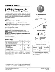
4. 1N5913B Series 3 W DO 41 Surmetic 30 Zener Voltage Regulators This is a complete series of 3 W Zener diodes with limits and excellent operating characteristics that reflect the superior capabilities of silicon oxide passivated junctions All this in an axial lead transfer molded plastic package that offers protection in all common environmental conditions Features e Zener Voltage Range 3 3 V to 200 V e ESD Rating of Class 3 gt 16 KV per Human Body Model e Surge Rating of 98 W 1 ms e Maximum Limits Guaranteed on up to Six Electrical Parameters Package No Larger than the Conventional 1 W Package Pb Free Packages are Available Mechanical Characteristics CASE Void free transfer molded thermosetting plastic FINISH external surfaces are corrosion resistant and leads are readily solderable MAXIMUM LEAD TEMPERATURE FOR SOLDERING PURPOSES 260 C 1 16 from the case for 10 seconds POLARITY Cathode indicated by polarity band MOUNTING POSITION Any MAXIMUM RATINGS Rams sms vae oni Max Steady State Power Dissipation 3 W 75 C Lead Length 3 8 Derate above 75 24 mW C Steady State Power Dissipation 1 W 50 Derate above 50 6 67 mW C Operating and Storage Ty Tstg 65 to Temperature Range 200 Maximum ratings are those values beyond which device damage can occur Maximum ratings applied to the device are individual stress limit values not normal operating
5. conditions and are not valid simultaneously If these invite are exceeded device functional operation is not implied damage may occur and reliability may be affected For additional information on our Pb Free strategy and soldering details please download the ON Semiconductor Soldering and Mounting Techniques Reference Manual SOLDERRM D Semiconductor Components Industries LLC 2006 1 April 2006 Rev 5 ON Semiconductor http onsemi com 9 M 4 o Cathode Anode AXIAL LEAD CASE 59 PLASTIC STYLE 1 MARKING DIAGRAM A Assembly Location 1N59xxB Device Number YY Year WW Work Week H Pb Free Package Note Microdot may be in either location ORDERING INFORMATION za rece 1N59xxB G Axial Lead Pb Free 1N59xxBRL G Axial Lead Pb Free TFor information on tape and reel specifications including part orientation and tape sizes please refer to our Tape and Reel Packaging Specification Brochure BRD8011 D Publication Order Number 1N5913B D ELECTRICAL CHARACTERISTICS TL 30 C unless otherwise noted Ve 1 5 V Max Ir 200 mAdc for all types Parameter Vz Reverse Zener Voltage 9 Iz 1N5913B Series Reverse Current Maximum Zener Impedance Iz Reverse Current Zzk Maximum Zener Impedance Izk Reverse Leakage Current Vn IR Vn Breakdown Voltage Zener Voltage Regulator Ve
6. horized use even if such claim alleges that SCILLC was negligent regarding the design or manufacture of the part SCILLC is an Equal Opportunity Affirmative Action Employer This literature is subject to all applicable copyright laws and is not for resale in any manner PUBLICATION ORDERING INFORMATION LITERATURE FULFILLMENT American Technical Support 800 282 9855 Toll Free ON Semiconductor Website http onsemi com Literature Distribution Center for ON Semiconductor USA Canada P O Box 61312 Phoenix Arizona 85082 1312 USA Order Literature http www onsemi coml litorder Phone 480 829 7710 or 800 344 3860 Toll Free USA Canada Japan ON Semiconductor Japan Customer Focus Center A Ma Fax 480 829 7709 or 800 344 3867 Toll Free USA Canada 2 9 1 Kamimeguro Meguro ku Tokyo Japan 153 0051 For additional information please contact your Email orderlit onsemi com Phone 81 3 5773 3850 local Sales Representative 1N5913B D
7. http onsemi com 2 1N5913B Series ELECTRICAL CHARACTERISTICS T 30 C unless otherwise noted Vp 1 5 V Max Ir 200 mAdc for all types Zener Voltage Note 2 Zener Impedance Note 3 Leakage Current sevice 1 Vz Volts 1 454 1N5913B G 1N5913B S 500 100 1N5917B G 1N5917B 4 500 5 1359198 1 5919 250 5 1N5920B G 1N5920B 200 5 1N5921B G 1N5921B 200 5 5 5 5 1N5923B G 1N5923B 1N5924B G 1N5924B 1N5925B G 1N5925B 1N5926B G 1N5926B 1N5927B G 1N5927B 1N5929B G 1N5929B 1N5930B G 1N5930B 1N5931B G 1N5931B 1N5932B G 1N5932B 1N5933B G 1N5933B 1N5934B G 1N5934B 1N5935B G 1N5935B 1N5936B G 1N5936B 1N5937B G 1N5937B 1N5938B G 1N5938B 1N5940B G 1N5940B 1N5941B G 1N5941B 1N5942B G 1N5942B 1N5943B G 1N5943B 1N5944B G 1N5944B 1 1 1 1 1 1 1 1 1 1 1 1 1 1 1 1 1 1N5946B 1 5946 1 1 5947 1 5947 1 1N5948B 1 5948 1 1N5950B 1 5950 1 1 1 1 1 1 1 1 5951 1 5951 EN 1 5952 1 5952 2 9 1N5953B 1N5953B 2 5 1N5954B G 1N5954B 2 3 1N5955B G 1N5955B Devices listed in bold italic are ON Semiconductor Preferred devices Preferred devices are recommended choices for future use and best overall value TThe G suffix indicates Pb Free package available 1 TOLERANCE AND TYPE NUMBER DESIGNATION Tolerance designation device tolerance of 5 are indicated by a B suffix 2 ZENER VOLTAGE Vz
8. igure 8 Vz 12 thru 82 Volts 10 2 80 9 70 5 o N c 2 50 z 1 amp j 40 je Loe E 30 a z 0 5 1 E L E PRIMARY PATH OF 02 10 CONDUCTION IS THROUGH 5 THE CATHODE LEAD 0 1 5 0 100 150 200 250 300 350 400 moon 1 8 1 4 3 8 12 5 8 3 4 7 8 1 c Vz ZENER VOLTAGE VOLTS Figure 9 Vz 100 thru 400 Volts http onsemi com 6 L LEAD LENGTH TO HEAT SINK INCH Figure 10 Typical Thermal Resistance POLARITY INDICATOR OPTIONAL AS NEEDED SEE STYLES 1N5913B Series PACKAGE DIMENSIONS AXIAL LEAD CASE 59 10 ISSUE U D NOTES 1 DIMENSIONING AND TOLERANCING PER ANSI Y14 5M 1982 JEDEC DO 41 OUTLI as DIMENSION CONTROLLING DIMENSION INCH ALL RULES AND NOTES ASSOCIATED WITH INE SHALL APPLY POLARITY DENOTED BY CATHODE BAND LEAD DIAMETER NOT CONTROLLED WITHIN F INCHES MILLIMETERS DIM MIN MAX MIN MAX 0 161 0 205 4 10 5 20 0 079 0 106 2 00 2 70 0 028 0 034 0 71 0 86 0 050 1 27 1 000 2540 STYLE 1 PIN 1 CATHODE POLARITY BAND 2 ANODE http onsemi com 7 1N5913B Series SURMETIC is a trademark of Semiconductor Components Industries LLC SCILLC ON Semiconductor and are registered trademarks of Semiconductor Components Industries LLC SCILLC SCILLC reserves the right to make changes without further notice to any products he
9. ious clips and tie points in common use and for printed circuit board wiring The temperature of the lead can also be measured using a thermocouple placed on the lead as close as possible to the tie point The thermal mass connected to the tie point is normally large enough so that it will not significantly respond to heat surges generated in the diode as a result of pulsed operation once steady state conditions are achieved Using the measured value of T the junction temperature may be determined by TL AT is the increase in junction temperature above the lead temperature and may be found from Figure 2 for a train of power pulses L 3 8 inch or from Figure 10 for dc power ATL Pp For worst case design using expected limits of Iz limits of Pp and the extremes of may be estimated Changes in voltage Vz can then be found from AV yz Oyz the zener voltage temperature coefficient is found from Figures 5 and 6 Under high power pulse operation the zener voltage will vary with time and may also be affected significantly by the zener resistance For best regulation keep current excursions as low as possible Data of Figure 2 should not be used to compute surge capability Surge limitations are given in Figure 3 They are lower than would be expected by considering only junction temperature as current crowding effects cause temperatures to be extremely high in small spots resulting in
10. rein SCILLC makes no warranty representation or guarantee regarding the suitability of its products for any particular purpose nor does SCILLC assume any liability arising out of the application or use of any product or circuit and specifically disclaims any and all liability including without limitation special consequential or incidental damages Typical parameters which may be provided in SCILLC data sheets and or specifications can and do vary in different applications and actual performance may vary over time All operating parameters including Typicals must be validated for each customer application by customer s technical experts SCILLC does not convey any license under its patent rights nor the rights of others SCILLC products are not designed intended or authorized for use as components in systems intended for surgical implant into the body or other applications intended to support or sustain life or for any other application in which the failure of the SCILLC product could create a situation where personal injury or death may occur Should Buyer purchase or use SCILLC products for any such unintended or unauthorized application Buyer shall indemnify and hold SCILLC and its officers employees subsidiaries affiliates and distributors harmless against all claims costs damages and expenses and reasonable attorney fees arising out of directly or indirectly any claim of personal injury or death associated with such unintended or unaut
Download Pdf Manuals

Related Search
ON SEMICONDUCTOR 1N5913B Series handbook