TEXAS INSTRUMENTS CD54HC32 CD74HC32 CD54HCT32 CD74HCT32 handbook
Contents
1. 7 0 020 0 51 0 012 0 31 10 010 0 25 4 Pin 1 Index Area 0 050 1 27 L 0 069 1 75 Max 7 0 004 0 10 Gauge Plane Seating Plane 0 010 0 25 4040047 3 H 11 2006 NOTES All linear dimensions ore in inches millimeters This drawing is subject to change without notice Body length does not include mold flash protrusions or gate burrs Mold flash protrusions or gate burrs shall not exceed 006 0 15 per end Body width does not include interlead flash Interlead flash shall not exceed 017 0 43 per side Reference JEDEC 5 012 variation AB mE EB 35 TEXAS INSTRUMENTS www ti com MECHANICAL DATA N R PDIP T PLASTIC DUAL IN LINE PACKAGE 16 PINS SHOWN PINS DIM A MAX A MIN MS 001 VARIATION 0 020 MIN 0 015 0 38 00 5 08 Cau x ge Plane l Seating Plane 125 3 18 MIN gt 4 0 010 0 25 NOM d 0 430 10 92 MAX D MAX 7 0 51 0 2 1 0 38 0 010 0 25 4 14 18 Pin Only 20 Pin vendor option A 4040049 E 12 2002 NOTES All linear dimensions are in inches millimeters This drawing is subject to change without notice Falls within JEDEC 5 001 except 182. CU NIPDAU Level 1 260C UNLIM no Sb Br CD74HC32M96E4 ACTIVE SOIC D 14 2500 Green RoHS amp NIPDAU Level 1 260C UNLIM no Sb Br CD74HC32M96G4 ACTIVE SOIC D 14 2500 Green RoHS amp NIPDAU Level 1 260C UNLIM no Sb Br CD74HC32ME4 ACTIVE SOIC D 14 50 Green RoHS amp NIPDAU Level 1 260C UNLIM no Sb Br CD74HC32MG4 ACTIVE SOIC D 14 50 Green RoHS amp NIPDAU Level 1 260C UNLIM no Sb Br CD74HC32MT ACTIVE SOIC D 14 250 Green RoHS amp NIPDAU Level 1 260C UNLIM no Sb Br CD74HC32MTE4 ACTIVE SOIC D 14 250 Green RoHS amp NIPDAU Level 1 260C UNLIM no Sb Br CD74HC32MTG4 ACTIVE SOIC D 14 250 Green RoHS amp NIPDAU Level 1 260C UNLIM no Sb Br CD74HCT32E ACTIVE PDIP N 14 25 Pb Free CU NIPDAU for Pkg Type RoHS CD74HCT32EE4 ACTIVE PDIP N 14 25 Pb Free CU NIPDAU N A for Pkg Type RoHS CD74HCT32M ACTIVE SOIC D 14 50 Green RoHS amp NIPDAU Level 1 260C UNLIM no Sb Br CD74HCT32M96 ACTIVE SOIC D 14 2500 Green RoHS amp CU NIPDAU Level 1 260C UNLIM no Sb Br CD74HCT32M96E4 ACTIVE SOIC D 14 2500 Green RoHS amp NIPDAU Level 1 260C UNLIM no Sb Br CD74HCT32M96G4 ACTIVE SOIC D 14 2500 Green RoHS amp NIPDAU Level 1 260C UNLIM no Sb Br CD74HCT32ME4 ACTIVE SOIC D 14 50 Green RoHS amp NIPDAU Level 1 260C UNLIM no Sb Br CD74HCT32MG4 ACTIVE SOIC D 14 50 Green RoHS amp NIPDAU Level 1 260C UNLIM no Sb Br CD74HCT32MT ACTIVE SOIC D 14 250 Green RoHS amp
3. Buyers acknowledge and agree that if they use any non designated products in automotive applications TI will not be responsible for any failure to meet such requirements Following are URLs where you can obtain information on other Texas Instruments products and application solutions Products Applications Amplifiers amplifier ti com Audio www ti com audio Data Converters dataconverter ti com Automotive www ti com automotive DSP dsp ti com Broadband www ti com broadband Clocks and Timers www ti com clocks Digital Control www ti com digitalcontrol Interface interface ti com Medical www ti com medical Logic logic ti com Military www ti com military Power Mgmt power ti com Optical Networking www ti com opticalnetwork Microcontrollers microcontroller ti com Security www ti com security RFID www ti rfid com Telephony www ti com telephony RF IF ZigBee Solutions www ti com Iprf Video amp Imaging www ti com video Wireless www ti com wireless Mailing Address Texas Instruments Post Office Box 655303 Dallas Texas 75265 Copyright 2008 Texas Instruments Incorporated
4. NIPDAU Level 1 260C UNLIM no Sb Br CD74HCT32MTE4 ACTIVE SOIC D 14 250 Green RoHS amp NIPDAU Level 1 260C UNLIM no Sb Br CD74HCT32MTG4 ACTIVE SOIC D 14 250 Green RoHS amp NIPDAU Level 1 260C UNLIM no Sb Br Addendum Page 1 9 Texas PACKAGE OPTION ADDENDUM INSTRUMENTS www ti com 9 Oct 2007 The marketing status values are defined as follows ACTIVE Product device recommended for new designs LIFEBUY TI has announced that the device will be discontinued and a lifetime buy period is in effect NRND Not recommended for new designs Device is in production to support existing customers but TI does not recommend using this part in a new design PREVIEW Device has been announced but is not in production Samples may or may not be available OBSOLETE TI has discontinued the production of the device 2 Eco Plan The planned eco friendly classification Pb Free RoHS Pb Free RoHS Exempt or Green RoHS amp no Sb Br please check http Awww ti com productcontent for the latest availability information and additional product content details TBD The Pb Free Green conversion plan has not been defined Pb Free RoHS TI s terms Lead Free or Pb Free mean semiconductor products that are compatible with the current RoHS requirements for all 6 substances including the requirement that lead not exceed 0 196 by weight in homogeneous materials Where designed to be soldered at high temperatures TI Pb Free pro
5. Page 2 J R G DIP Tx 14 LEADS SHOWN CERAMIC DUAL IN LINE PACKAG B nnmnmnmnmnn Ra SUARUM 0 065 1 65 0 045 1 14 0 005 0 13 MIN 0 026 0 66 0 014 0 36 0 100 2 54 PINS B 14 16 18 20 gt 0 300 0 300 0 300 0 300 A 7 62 7 62 7 62 7 62 BSC BSC BSC BSC ET 0 785 840 0 960 1 060 19 24 21 34 24 38 26 92 C B MIN 0 300 0 300 0 310 0 300 7 62 7 62 7 87 7 62 EAN 0 245 0 245 0 220 0 245 6 22 6 22 5 59 6 22 0 060 1 52 0 015 0 38 0 200 5 08 MAX n Y Seating Plane 1 0 130 3 30 MIN U U ke 0 15 0 014 0 36 4040083 F 03 03 NOTES All linear dimensions are in inches millimeters This drawing is subject to change without notice This package is hermetically sealed with a ceramic lid using glass frit Index point is provided on cap for terminal identification only on press ceramic glass frit seal only Falls within MIL STD 1835 GDIP1 7T14 GDIP1 T16 GDIP1 T18 and GDIP1 T20 MECHANICAL DATA D R PDSO C14 PLASTIC SMALL OUTLINE PACKAGE
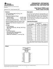
6. 35 TEXAS INSTRUMENTS Data sheet acquired from Harris Semiconductor SCHS274C September 1997 Revised September 2003 Features Typical Propagation Delay 7ns at Vcc 5V C 15pF TA 25 C Fanout Over Temperature Range Standard Outputs Bus Driver Outputs 10 LSTTL Loads 15 LSTTL Loads Wide Operating Temperature Range 55 C to 125 C Balanced Propagation Delay and Transition Times Significant Power Reduction Compared to LSTTL Logic ICs HC Types 2V to 6V Operation High Noise Immunity Ny 30 30 of Vcc at Vcc 5V HCT Types 4 5V to 5 5V Operation Direct LSTTL Input Logic Compatibility Vip 0 8V Max 2V Min CMOS Input Compatibility lt 14A at VoL Pinout CD54HC32 CD74HC32 CD54HCT32 CD74HCT32 High Speed CMOS Logic Quad 2 Input OR Gate Description The HC32 and HCT32 contain four 2 input OR gates in one package Logic gates utilize silicon gate CMOS technology to achieve operating speeds similar to LSTTL gates with the low power consumption of standard CMOS integrated cir cuits All devices have the ability to drive 10 LSTTL loads The HCT logic family is functionally pin compatible with the standard LS logic family Ordering Information TEMP RANGE PART NUMBER c PACKAGE CD54HCT32F3A 5510125 14 Ld CERDIP CD74HC32M 55 to 125 CD74HC32MT 55 to 125 CD74HC32M96 55 to 125 CD74HCT32E 55 to 125 CD74HCT32M 55 to 125 CD74HCT32MT 5
7. 5 to 125 14 Ld SOIC 14 Ld SOIC NOTE When ordering use the entire part number The suffix 96 denotes tape and reel The suffix T denotes a small quantity reel of 250 CD74HCT32M96 55 to 125 CD54HC32 CD54HCT32 CERDIP CD74HC32 CD74HCT32 PDIP SOIC TOP VIEW CAUTION These devices are sensitive to electrostatic discharge Users should follow proper IC Handling Procedures Copyright 2003 Texas Instruments Incorporated CD54HC32 CD74HC32 CD54HCT CD74HCT32 Functional Diagram TRUTH TABLE H High Voltage Level L Low Voltage Level HC Logic Symbol HCT Logic Symbol CD54HC32 CD74HC32 CD54HCT CD74HCT32 Absolute Maximum Ratings Thermal Information DC Supply Voltage Vcc 0 5V to 7V Thermal Resistance Typical Note 1 DC Input Diode Current E PDIP Package For Vj lt 0 5V or Vi gt Veg 0 5 20mA M SOIC Package DC Output Diode Current lox Maximum Junction Temperature Hermetic Package or Die For Vo lt 0 5V gt 0 5 20mA Maximum Junction Temperature Plastic Package DC Output Source or Sink Current per Output Pin Io Maximum Storage Temperature Range For Vo gt 0 5V lt 0 5 25mA Maximum Lead Temperature Soldering 10s DC or Ground Current loc or IGND 50 SOIC Lead Tips Only Operating Conditions Temperature Range Ta 559C to 1259C
8. Supply Voltage Range Vcc HC Types 2V to 6V HET Types rre m Rhen 4 5V to 5 5V DC Input or Output Voltage Vi Vo Input Rise and Fall Time 1000ns Max 500ns Max 400ns Max CAUTION Stresses above those listed in Absolute Maximum Ratings may cause permanent damage to the device This is a stress only rating and operation of the device at these or any other conditions above those indicated in the operational sections of this specification is not implied NOTE 1 The package thermal impedance is calculated in accordance with JESD 51 7 DC Electrical Specifications TEST CONDITIONS 409 TO 859C 559 TO 1259 PARAMETER SYMBOL Vcc V UNITS Fue Tue m wax m nes LC TSDTCLDSICLDEI ILe s es T fos fos LL Pe ee e HC TYPES High Level Input Voltage I lt lt lt lt Low Level Input Voltage High Level Output 0 02 Voltage CMOS Loads qele Lolo N rnm High Level Output Voltage TTL Loads Low Level Output 0 02 Voltage CMOS Loads Low Level Output Voltage TTL Loads Quiescent Device Current 5 gt CD54HC32 CD74HC32 CD54HCT32 CD74HCT32 DC Electrical Specifications Continued TEST CONDITIONS 409 TO 859C 559 TO 1259 PARAMETER SYMBOL Vcc V UNITS uo e ees EM HCT TYPES High Level Input 4 5 to Voltage 5 5 Low Level Input 4 5 to Voltage 5 5 High Level Ou
9. and 20 pin minimum body length Dim The 20 pin end lead shoulder width is a vendor option either half or full width bp o gt 35 TEXAS INSTRUMENTS www ti com IMPORTANT NOTICE Texas Instruments Incorporated and its subsidiaries reserve the right to make corrections modifications enhancements improvements and other changes to its products and services at any time and to discontinue any product or service without notice Customers should obtain the latest relevant information before placing orders and should verify that such information is current and complete All products are sold subject to Tl s terms and conditions of sale supplied at the time of order acknowledgment TI warrants performance of its hardware products to the specifications applicable at the time of sale in accordance with Tl s standard warranty Testing and other quality control techniques are used to the extent TI deems necessary to support this warranty Except where mandated by government requirements testing of all parameters of each product is not necessarily performed TI assumes no liability for applications assistance or customer product design Customers are responsible for their products and applications using Tl components To minimize the risks associated with customer products and applications customers should provide adequate design and operating safeguards TI does not warrant or represent that any license either express or implied is gr
10. anted under any TI patent right copyright mask work right or other TI intellectual property right relating to any combination machine or process in which TI products or services are used Information published by TI regarding third party products or services does not constitute a license from TI to use such products or services or a warranty or endorsement thereof Use of such information may require a license from a third party under the patents or other intellectual property of the third party or a license from TI under the patents or other intellectual property of TI Reproduction of TI information in TI data books or data sheets is permissible only if reproduction is without alteration and is accompanied by all associated warranties conditions limitations and notices Reproduction of this information with alteration is an unfair and deceptive business practice is not responsible or liable for such altered documentation Information of third parties may be subject to additional restrictions Resale of TI products or services with statements different from or beyond the parameters stated by TI for that product or service voids all express and any implied warranties for the associated product or service and is an unfair and deceptive business practice TI is not responsible or liable for any such statements TI products are not authorized for use in safety critical applications such as life support where a failure of the TI product wou
11. ducts are suitable for use in specified lead free processes Pb Free RoHS Exempt This component has a RoHS exemption for either 1 lead based flip chip solder bumps used between the die and package or 2 lead based die adhesive used between the die and leadframe The component is otherwise considered Pb Free RoHS compatible as defined above Green RoHS amp no Sb Br TI defines Green to mean Pb Free RoHS compatible and free of Bromine Br and Antimony Sb based flame retardants Br or Sb do not exceed 0 196 by weight in homogeneous material 3 MSL Peak Temp The Moisture Sensitivity Level rating according to the JEDEC industry standard classifications and peak solder temperature Important Information and Disclaimer The information provided on this page represents TI s knowledge and belief as of the date that it is provided TI bases its knowledge and belief on information provided by third parties and makes no representation or warranty as to the accuracy of such information Efforts are underway to better integrate information from third parties has taken and continues to take reasonable steps to provide representative and accurate information but may not have conducted destructive testing or chemical analysis on incoming materials and chemicals and TI suppliers consider certain information to be proprietary and thus CAS numbers and other limited information may not be available for release In no event shall TI s l
12. iability arising out of such information exceed the total purchase price of the TI part s at issue in this document sold by to Customer on an annual basis Addendum Page 2 X3 Texas PACKAGE MATERIALS INFORMATION INSTRUMENTS www ti com 11 Mar 2008 TAPE AND REEL INFORMATION REEL DIMENSIONS TAPE DIMENSIONS A Reel Diameter Dimension designed to accommodate the component width Dimension designed to accommodate the component length Dimension designed to accommodate the component thickness y Overall width of the carrier tape Y Pitch between successive cavity centers t Reel Width W1 QUADRANT ASSIGNMENTS FOR PIN 1 ORIENTATION IN TAPE Sprocket Holes User Direction of Feed All dimensions are nominal Device Package SPQ Reel Reel 0 mm KO mm P1 Pin1 Type Drawing Diameter Width mm mm Quadrant mm W1 mm CD74HC32M96 SOIC D 14 2500 330 0 16 4 6 5 9 0 2 1 8 0 16 0 Q1 CD74HCT32M96 SOIC D 14 2500 330 0 16 4 6 5 9 0 2 1 8 0 16 0 Q1 Pack Materials Page 1 X3 Texas PACKAGE MATERIALS INFORMATION INSTRUMENTS www ti com 11 Mar 2008 TAPE AND REEL BOX DIMENSIONS All dimensions are nominal Device Package Type Drawing Pins SPQ Length mm Width mm Height mm CD74HC32M96 SOIC D 14 2500 346 0 346 0 33 0 CD74HCT32M96 SOIC D 14 2500 346 0 346 0 33 0 Pack Materials
13. ld reasonably be expected to cause severe personal injury or death unless officers of the parties have executed an agreement specifically governing such use Buyers represent that they have all necessary expertise in the safety and regulatory ramifications of their applications and acknowledge and agree that they are solely responsible for all legal regulatory and safety related requirements concerning their products and any use of TI products in such safety critical applications notwithstanding any applications related information or support that may be provided by TI Further Buyers must fully indemnify TI and its representatives against any damages arising out of the use of TI products in such safety critical applications TI products are neither designed nor intended for use in military aerospace applications or environments unless the TI products are specifically designated by TI as military grade or enhanced plastic Only products designated by TI as military grade meet military specifications Buyers acknowledge and agree that any such use of TI products which TI has not designated as military grade is solely at the Buyer s risk and that they are solely responsible for compliance with all legal and regulatory requirements in connection with such use TI products are neither designed nor intended for use in automotive applications or environments unless the specific products are designated by as compliant with ISO TS 16949 requirements
14. to CL 15pF Output Y Transition Times Figure 2 m trHL ncn 50pF 4 45 Input Capacitance Input Capacitance 10 pO Power Dissipation Notes 3 4 NOTES 3 Cpp is used to determine the dynamic power consumption per gate 4 Vec fi Cpp CL where fj Input Frequency C Output Load Capacitance Vcc Supply Voltage Test Circuits and Waveforms INVERTING INVERTING OUTPUT OUTPUT FIGURE 1 HC AND HCU TRANSITION TIMES AND PROPAGA FIGURE 2 HCT TRANSITION TIMES AND PROPAGATION TION DELAY TIMES COMBINATION LOGIC DELAY TIMES COMBINATION LOGIC X3 Texas PACKAGE OPTION ADDENDUM INSTRUMENTS www ti com 9 Oct 2007 PACKAGING INFORMATION Orderable Device Status Package Package Pins Package Eco Plan Lead Ball Finish MSL Peak Temp Type Drawing Qty 5962 8685201CA ACTIVE CDIP J 14 1 TBD A42 SNPB N A for Pkg Type CD54HC32F3A ACTIVE CDIP J 14 1 TBD A42 SNPB N A for Pkg Type CD54HCT32F ACTIVE CDIP J 14 1 TBD A42 SNPB N A for Pkg Type CD54HCT32F3A ACTIVE CDIP J 14 1 TBD A42 SNPB N A for Pkg Type CD74HC32E ACTIVE PDIP N 14 25 Pb Free NIPDAU for Pkg Type RoHS CD74HC32bE4 ACTIVE PDIP N 14 25 Pb Free CU NIPDAU N A for Pkg Type RoHS CD74HC32M ACTIVE SOIC D 14 50 Green RoHS amp NIPDAU Level 1 260C UNLIM no Sb Br CD74HC32M96 ACTIVE SOIC D 14 2500 Green RoHS amp
15. tput Voltage CMOS Loads High Level Output Voltage TTL Loads Low Level Output Voltage CMOS Loads Low Level Output Voltage TTL Loads Input Leakage Current Quiescent Device Current Additional Quiescent Device Current Per Input Pin 1 Unit Load NOTE 2 For dual supply systems theoretical worst case Vj 2 4V 5 5V specification is 1 8mA HCT Input Loading Table NOTE Unit Load is Alcc limit specified in DC Electrical Specifications table e g 360A max at 25 C Switching Specifications Input ty t 6ns 5 LU m A A ENT Propagation Delay Input to CL 50pF 15 ns EIER DERE SUM Propagation Delay Data Inputto CL 15pF Output Y Transition Times Figure 1 CL 50pF 11 arm a m ER E Res CD54HC32 CD74HC32 CD54HCT CD74HCT32 Switching Specifications Input t t 6ns Continued PARAMETER SYMBOL CONDITIONS V MIN TYP MAX MIN MAX MIN MAX UNITS Power Dissipation Capacitance Cpp 5 22 pF Notes 3 4 HCT TYPES Propagation Delay Input to CL 50pF 4 5 24 30 36 ns Output Figure 2 Propagation Delay Data Input
Download Pdf Manuals

Related Search
TEXAS INSTRUMENTS CD54HC32 CD74HC32 CD54HCT32 CD74HCT32 handbook