SUPERTEX TP2520 TP2522 DATA SHEET
Contents
1. Notes 1 All D C parameters 100 tested at 25 C unless otherwise stated Pulse test 300us pulse 2 duty cycle 2 All A C parameters sample tested Switching Waveforms and Test Circuit ov PULSE INPUT Se Ee o E 1l l l 10V l E l l tuorry te D U T l ov l INPUT l 9 OUTPUT l l OUTPUT l l R Vop SS Sie l TP2520 TP2522 Typical Performance Curves Output Characteristics Saturation Characteristics T g g oO 0 a a E E o s 2 Vps volts Transconductance vs Drain Current Power Dissipation vs Ambient Temperature 1 0 2 0 Vos 25V TO 243AA 0 8 T x Ta 55 C g 5 i E D o 0 4 ee a fol Ta 25 C 4 m mm X A T 12500 N M 0 2 A ENS 4 SN SN 0 0 0 0 4 0 8 1 2 1 6 2 0 0 25 50 75 100 125 150 lp amperes T4 C Maximum Rated Safe Operating Area Thermal Response Characteristics 10 Ta 25 C o 0 N TO 243AA pulsed a a m E 40 o g S 0 oO BA 2 eo E 8 p d G TE TO 243AA TO 243AA DC l E Ta 25 C 2 Pp 1 6W Lr 0 01 1 10 100 1000 0 001 0 01 0 1 1 10 Vps volts tp2. process This combination produces devices with the power handling capabilities of bipolar transis tors and with the high input impedance and positive temperature coefficient inherent in MOS devices Characteristic of all MOS structures these devices are free from thermal runaway and thermally induced secondary breakdown Supertex s vertical DMOS FETs are ideally suited to a wide range of switching and amplifying applications where very low threshold voltage high breakdown voltage high input impedance low input capacitance and fast switching speeds are desired Package Option D G D S TO 243AA SOT 89 Note See Package Outline section for dimensions Supertex Inc does not recommend the use of its products in life support applications and will not knowingly sell its products for use in such applications unless it receives an adequate products liability indemnification insurance agreement Supertex does not assume responsibility for use of devices described and limits its liability to the replacement of devices determined to be defective due to workmanship No responsibility is assumed for possible omissions or inaccuracies Circuitry and specifications are subject to change without notice For the latest product specifications refer to the Supertex website http www supertex com For complete liability information on all Supertex products refer to the most current databook or to the Legal Disclaimer page on the Supertex w
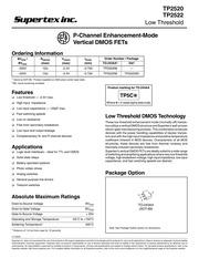
3. Supertex inc TP2520 TP2522 Low Threshold P Channel Enhancement Mode Vertical DMOS FETs Ordering Information BVpss Roscon Vas Ibon BVpas max max min 200V 12Q 2 4V 0 75A Order Number Package TO 243AA Diet TP2520N8 e 220V 122 2 4V 0 75A Same as SOT 89 Product supplied on 2000 piece carrier tape reels MIL visual screening available Features T Low threshold 2 4V max Q High input impedance Q Low input capacitance 125pF max 1 Fast switching speeds 1 Low on resistance 1 Free from secondary breakdown 1 Low input and output leakage Q Complementary N and P channel devices Applications Logic level interfaces ideal for TTL and CMOS Solid state relays Battery operated systems Photo voltaic drives Analog switches General purpose line drivers ODC CODO O Telecom switches Absolute Maximum Ratings Drain to Source Voltage BVpss Drain to Gate Voltage BVpas Gate to Source Voltage 20V Operating and Storage Temperature 55 C to 150 C Soldering Temperature 300 C Distance of 1 6 mm from case for 10 seconds 11 12 01 TP2522N8 TP2522ND Product marking for TO 243AA TP5C Where 2 week alpha date code Low Threshold DMOS Technology These low threshold enhancement mode normally off transis tors utilize a vertical DMOS structure and Supertex s well proven silicon gate manufacturing
4. ebsite TP2520 TP2522 Thermal Characteristics Package Ip continuous Ip pulsed Power Dissipation ic Oja Ta 25 C C W C W 15 78t TO 243AA 260mA 2 0A 1 6W continuous is limited by max rated T t Mounted on FR5 board 25mm x 25mm x 1 57mm Significant P increase possible on ceramic substrate Electrical Characteristics 25 C unless otherwise specified Parameter i Conditions Drain to Source Breakdown Voltage Fegse Ves OV Ip 2mA TP2520 Vas Gate Threshold Voltage Vas Vps lp 1mA AVesith Change in Veg p with Temperature Ves Vps Ip 1mA less Gate Body Leakage Ves 20V Vps OV Ipss Zero Gate Voltage Drain Current Ves OV Vps Max Rating Ves OV Vps 0 8 Max Rating T 125 C Ip oN ON State Drain Current Ves 4 5V Vps 25V Ves 1 OV Vos 25V Static Drain to Source Vag 4 5V Ip 100mA ON State Resistance Vas 10V Ip 200mA Change in Rogon with Temperature Ves 10V Ip 200mA Forward Transconductance Vbs 25V Ip 200mA Input Capacitance Ves OV Vps 25V Common Source Output Capacitance f 1 MHz Reverse Transfer Capacitance Turn ON Delay Time Rise Time Vpp 25V o lp 0 75A Turn OFF Delay Time y Reen 252 Fall Time Diode Forward Voltage Drop Ves OV Isp 0 5A Reverse Recovery Time Ves OV lsp 0 5A
5. seconds TP2520 TP2522 Typical Performance Curves BVpss Variation with Temperature On Resistance vs Drain Current 1 1 1 0 BVpss normalized Roson ohms 0 9 0 0 5 1 0 1 5 2 0 2 5 Ip amperes Vin and Rpg Variation with Temperature 25 2 0 2 c o 3 g I o 15 W o Z E E E e 2 S p 10 2 zo o 0 5 0 50 0 50 100 150 Ves volts T C Capacitance vs Drain to Source Voltage Gate Drive Dynamic Characteristics 200 150 g z E 2 G 100 2 2 2 amp gt O 50 0 0 0 5 1 0 1 5 2 0 2 5 Vps volts Qa nanocoulombs 11 12 01 Sur e ex inc 1235 Bordeaux Drive Sunnyvale CA 94089 p TEL 408 744 0100 FAX 408 222 4895 2001 Supertex Inc All rights reserved Unauthorized use or reproduction prohibited www supertex com
Download Pdf Manuals

Related Search
SUPERTEX TP2520 TP2522 DATA SHEET