ANALOG DEVICES AD7306 English products handbook Rev B
Contents
1. Parameter Min Typ Max Units Test Conditions C omments RS 232 DRIVER TTL Input Logic Low V y 0 8 V TTL Input Logic High Viny 2 0 V Input Logic Current 0 1 10 uA Vin 0 V to Vec RS 232 High Level Output Voltage 5 0 7 3 V R 3kQ RS 232 Low Level Output Voltage 5 0 6 5 V R 3kQ Output Short Circuit C urrent 5 12 mA Vout 0V TA 0 C to 70 C Slew Rate 8 20 30 V us C 50 pF R 3kQ 4 V us C 2500 pF R 3 kQ Output Resistance Powered D own 300 10M Q Vec 0V Vout t3 V RS 232 RECEIVER Input Voltage Range 15 15 V RS 232 Input T hreshold Low 0 8 1 3 V RS 232 Input T hreshold H igh 1 7 2 4 V RS 232 Input H ysteresis 0 1 0 4 1 0 V RS 232 Input Resistance 3 5 7 kQ TTL Output Voltage Low Vo 0 2 0 4 V lour 4 mA TTL Output Voltage High Vox 3 5 4 8 V lour 4 MA RS 422 DRIVER TTL Input Logic Low V y 0 8 V TTL Input Logic High Viny 2 0 V Logic Input Current 0 1 10 uA Vin 0 V to Vec Differential Output Voltage 5 0 V Vcc 5 V R Diff eo Figure 3 2 V R Diff 100 Figure 3 Common M ode Output Voltage 3 V A Vout for Complementary O P States 0 2 V R Diff 100 Q Output Short Circuit Current 35 150 mA OV lt Vcmr S 7 V RS 422 RECEIVER Common M ode Voltage Range 7 V T ypical RS 422 Input Voltage lt 5 V Differential Input T hreshold Voltage 0 2 0 2 V Input Voltage H ysteresis 70 mV Vom 0V Input Resistance 3 5 7 ko TTL Output Voltage Low Vo 0 2 0 4 V lour 4 0 mA TTL Output Voltage High Vo2. ov T3 our A T3 our B tskew t SKEW Vi 9 90 POINT 90 POINT ov 10 POINT 10 POINT te Figure 4 RS 422 Driver Propagation Delay Rise Fall Timing DIFFERENTIAL INPUT R1 B RTN A 2 5V Rlour 232 422 SEL Rtour RS 232 RS 232 RS 422 Figure 6 RS 232 RS 422 Receiver Enable Timing AD7306 GENERAL DESCRIPTION T he AD 7306 drivers receivers provide an interface which is compatible with RS 232 RS 422 standard interfaces As both standards are widely accepted it is often necessary to provide an interface which is compatible with both T he AD 7306 is ideally suited to this type of application as both standards may be met using a single package T his part contains two RS 232 drivers one RS 422 driver one RS 232 receiver and one receiver path which can be configured as either RS 232 or RS 422 T his re ceiver is configured using the 232 422 SEL pin T his part also contains an internal charge pump voltage con verter which facilitates operation using a single 5 V power supply Charge Pump DC DC Voltage Generator T he charge pump voltage generator uses a switched capacitor technique to develop 10 V levels from an input 5 V supply A highly efficient charge pump design coupled with a high fre quency internal oscillator permit operation using four 0 1 uF capacitors 10V ae OUTPUT o POWER SUPPLY NEN O CC GENERATOR SUPPLY 10V OUTPUT Ci Ci C1 0 1uF c
3. 2 0 1uF Figure 7 Charge Pump Voltage Generator Capacitors C1 and C2 act as charge storage capacitors while C 3 and C4 provide output smoothing F or correct operation all four capacitors must be included Either polarized or nonpolarized capacitors may be used for C1 C4 If a polarized type is used then the correct polarity should be observed T his may be ig nored with nonpolarized type capacitors T he charge pump output voltages V and V are used inter nally to power the RS 232 transmitters T his permits RS 232 output levels to be developed on the RS 232 transmitter out puts T he charge pump output voltages may also be used to power external circuitry if the current requirements are small Please refer to the T ypical Performance Characteristics T he generator rise time after power up is 200 us typical T his time is necessary to completely charge the storage capacitors in the charge pump Therefore RS 232 data transmission should not be initiated until this time has elapsed after switch on T his will ensure that valid data is always transmitted RS 232 Drivers T he RS 232 drivers in the AD 7306 meet the EIA RS 232 specifications T he drivers are inverting level shifters which convert TT L CM OS levels into RS 232 output levels T he in put switching threshold is typically 1 3 V With a typical RS 232 load the output levels are 7 5 V Under worst case load conditions the drivers are guaranteed to provide 5 V which m
4. AL O P CURRENT mA Figure 9 RS 232 Driver Slew Rate vs Load Capacitance Figure 12 RS 422 Driver Output Current vs Output Voltage jim tt EZER KE EN PEN e ei el SACRE AAR Figure 10 RS 232 Driver R 5 kQ C 50 pF Figure 13 RS 422 Driver Ri pir 100 Q C C 2 100 pF REV B 7 AD7306 Single E nded Data Transmission Single ended interfaces are used for low speed short distance communications such as from a computer terminal to a printer A singleline is used to carry the signal Various standards have been developed to standardize the communication link the most popular of these being the RS 232 The RS 232 standard was introduced in 1962 by the EIA and has been widely used throughout the industry T he standard has been revised several times and the current revision is known as EIA 232E The RS 232 standard is suitable for single ended data transmission at relatively slow data rates over short distances A typical RS 232 interface is shown in Figure 14 DATA o o DATA IN OUT RS 232 CHANNEL Figure 14 Single Ended RS 232 Interface Differential Data Transmission When transmitting at high data rates over long distances and through noisy environments single ended data transmission is often inadequate In this type of application differential data transmission offers superior performance Differential transmis sion uses two signal lines to transmit data It rejects ground shifts and is insen
5. ANALOG DEVICES 5 V Powered RS 232 RS 422 Transceiver AD7306 FEATURES RS 232 and RS 422 on One Chip Single 5 V Supply 0 1 F Capacitors Short Circuit Protection Excellent Noise Immunity Low Power BiCMOS Technology High Speed Low Skew RS 422 Operation 40 C to 85 C Operations APPLICATIONS DTE DCE Interface Packet Switching Local Area Networks Data Concentration Data Multiplexers Integrated Services Digital Network ISDN GENERAL DESCRIPTION The AD 7306 line driver receiver isa 5 V monolithic product which provides an interface between TTL signal levels and dual standard EIA RS 232 RS 422 signal levels T he part contains two RS 232 drivers one RS 422 driver one RS 232 receiver and one receiver path which can be configured either as RS 232 or as RS 422 An internal charge pump voltage converter facilitates operation from a single 5 V power supply T he internal charge pump generates 10 V levels allowing RS 232 output levels to be de veloped without the need for external bipolar power supplies A highly efficient charge pump design allows operation using non polarized miniature 0 1 uF capacitors T his gives a consid erable saving in printed circuit board space over conventional products which can use up to 10 uF capacitors The charge pump output voltages may also be used to power external cir cuitry which requires dual supplies REV B Information furnished by Analog Devices is believed to b
6. BSC 24 Lead Pin Plastic DIP N 24 0 260 0 001 6 61 0 03 oe ae ee LY KP ap YP YP 0 32 8 128 0 30 7 62 1 228 31 19 i 1226 31 14 gt y m 0 130 3 30 0 128 3 25 j j j j j i E 0 009 0 23 ole leo A IE 0 15 0 02 0 5 0 016 0 41 0 11 2 79 0 09 2 28 0 07 1 78 0 05 1 27 NOTES 1 LEAD NO 1 IDENTIFIED BY DOT OR NOTCH 2 PLASTIC LEADS WILL BE EITHER SOLDER DIPPED OR TIN LEAD PLATED IN ACCORDANCE WITH MIL M 385 10 REQUIREMENTS REV B C1624a 2 8 94 PRINTED IN U S A
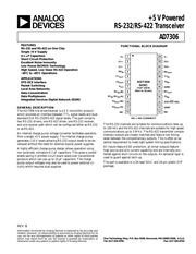
7. e accurate and reliable However no responsibility is assumed by Analog Devices for its use nor for any infringements of patents or other rights of third parties which may result from its use No license is granted by implication or otherwise under any patent or patent rights of Analog Devices FUNCTIONAL BLOCK DIAGRAM V 24 V C1 23 c2 c1 22 c2 R2 R2our Tour Tin T2our AD7306 T2in Vec SOIC GND TOP VIEW R1 B Not to Scale R1 out R1y R1 yy A T3in T3our B 232 422 SEL T3our A GND NC NC NC NO CONNECT T he RS 232 channels are suitable for communications rates up to 100 kHz and the RS 422 channels are suitable for high speed communications up to 5 M Hz T he RS 422 transmitter comple mentary outputs are closely matched and feature low timing skew between the complementary outputs T his is often an es sential reguirement to meet tight system timing specifications All inputs feature ESD protection all driver outputs feature high source and sink current capability and are internally pro tected against short circuits on the outputs An epitaxial layer is used to guard against latch up T he part is available in a 24 lead SOIC and 24 pin plastic DIP package One Technology Way P O Box 9106 Norwood MA 02062 9106 U S A Tel 617 329 4700 Fax 617 326 8703 AD7306 SPECIFICATIONS Vec 5 V 5 C1 C2 C3 C4 0 1 pF All specifications Ty to Tmax unless otherwise noted
8. e noted Toit s apas esas EY ek Lae Continuous Ve eaten alah cat GN Mae te Abani 7V Power Dissipation VA NN e a had Set tte Se tad Vcc 0 3 V to 13 2 V Small Outline 650 mW AVIS sa tava barnes sn dala neta turd at iat ala gel 0 3 V to 13 2 V DIP eee 650 mW Inputs Operating T emperature Range TI Ye ER ota ce V to V Commercial J Version 0 C to 70 C 1 e e elik aa tA 0 3 V to V Industrial A Version 40 C to 85 C R IN ATB R2iy g aa ila d aa auca 25 V to 25 V Storage T emperature Range 65 C to 150 C 232 422 GEM State cg tee el e 0 3V toV Lead Temperature Soldering 10 secs 300 C Outputs Stresses above those listed under Absolute Maximum Ratings may cause Tl tcl ZOU TS eck eet el a 15Vto 15 V permanent damage to the device This is a stress rating only and functional T3oo A B O Tees en ee a ee 0 3 V to Vcc 0 3 V LA S LS l maximum ratings for extended periods of time may affect device reliability CAUTION ESD electrostatic discharge sensitive device Electrostatic charges as high as 4000 V readily accumulate on the human body and test equipment and can discharge without detection WARNING S Although the AD 7306 features proprietary ESD protection circuitry permanent damage may At occur on devices subjected to high energy electrostatic discharges Therefore proper ESD precautions are recom
9. eets the minimum RS 232 requirement T he output slew rate is internally limited to lt 30 V us without the need for an external slew limiting capacitor Short circuit protection is also provided which prevents damage in the event of output fault conditions Active current limiting is used which limits the output short circuit current to less than 12 mA in the event of an output fault T his type of current limiting does not degrade the output voltage swing under normal loading conditions as would be the case with conventional passive limiting T he powered down output impedance is typically 10 MQ T his is considerably larger than the 300 minimum value required by the RS 232 specification It provides additional protection under fault conditions where another powered up transmitter output is inadvertently shorted to the powered down device RS 232 Receivers T he receivers are inverting level shifters which accept RS 232 input levels 3 V to 15 V and translates them into 5 V TTL CM OS levels T he input switching thresholds are 0 8 V minimum and 2 4 V maximum which are well within the RS 232 requirement of 3 V Internal 5 kQ pull down resistors to GND are provided on the receiver inputs T his ensures that an unconnected input will be interpreted as a low level giving a Logic 1 on the TTL CM OS output Excellent noise immu nity is achieved by the use of hysteresis and internal filtering circuitry T he filter rejects noise glitches
10. igures Receiver R1 to accept either RS 232 or RS 422 signal lev els A Logic 1 on this input selects 232 operation while a Logic 0 selects 422 operation 16 9 T3N TTL CMOS Input to the RS 422 T ransmitter T 3 17 10 Rlour TTL CMOS Output from Receiver R1 19 12 T2in TTL CM OS Input to RS 232 Transmitter T 2 20 13 T lin TTL CM OS Input to RS 232 Transmitter T 1 21 14 R2our TTL CMOS Output from Receiver R2 22 23 15 17 C2 C2 External Capacitor 2 T erminals A 0 1 uF capacitor must be connected between these pins 24 18 V Internally G enerated N egative Supply 9 V nominal A 0 1 uF capacitor must be connected between this pin and GND SOIC AD7306 SOIC TOP VIEW Not to Scale NC NO CONNECT PIN CONFIGURATIONS DIP AD7306 DIP TOP VIEW Not to Scale NC NO CONNECT REV B AD7306 5V INPUT O 0 1uF 0 1uF 10V H POWER SUPPLY 0 1uF 0 1uF GENERATOR TiN Tlour RS 232 TTUCMOS OUTPUTS INPUTS 12N Tour S 422 T3 N T3 out B output T3 out A RS 232 R2 our R2 n INPUT TTL CMOS OUTPUTS RS 232 R1 our R N R1N a RS 422 INPUT RS 422 RTN e INPUT 232 422 SEL O Figure 1 AD7306 Application Circuit T3 our B Cu 100pF T3N RL pr 1009 C a 100pF T3 out A Figure 2 RS 422 Driver Propagation Delay Test Circuit T3 out B gt Q T3 our A Figure 3 RS 422 Driver Voltage Measurement Test Circuit REV B 3V
11. mended to avoid performance degradation or loss of functionality ESD SENSITIVE DEVICE ORDERING GUIDE Model Temperature Range Package Description Package Option AD7306JR 0 C to 70 C 24 Lead SOIC R 24 AD7306JN 0 C to 70 C 24 PinDIP N 24 AD7306AR 40 C to 85 C 24 Lead SOIC R 24 AD7306AN 40 C to 85 C 24 Pin DIP N 24 REV B 3 PIN FUNCTION DESCRIPTION SOIC DIP Pin Pin Mnemonic Function 1 19 V Internally Generated Positive Supply 9 V nominal A 0 1 uF capacitor must be connected between this pin and GND 2 3 20 22 C1 C1 External Capacitor 1 T erminals A 0 1 uF capacitor must be connected between these pins 4 23 R2in RS 232 Receiver R2 Input T his input accepts RS 232 input voltages 5 24 T lout RS 232 Transmitter Driver T 1 Output Typically 7 5 V 6 1 T 2ourt RS 232 Transmitter Driver T 2 Output T ypically 7 5 V 7 2 Vec Power Supply Input 5 V 5 8 3 R1 B RS 422 Receiver RI Differential Input B 9 4 R1n Rl n A Receiver RI Input M ay be configured to accept either single ended RS 232 levels or differential RS 422 levels It is configured using the 232 422 SEL pin 10 5 T3our B RS 422 T ransmitter D river T 3 D ifferential Output B 11 6 T3our A RS 232 Transmitter Driver T 3 Differential Output A 12 13 16 21 NC No Connect Pins 14 18 7 11 GND Ground Pin M ust be connected to 0 V 15 8 232 422 SEL Select Input T his input conf
12. of up to 0 5 us in duration RS 422 Driver The RS 422 driver on the AD 7306 accepts aT TL CM OS in put and translates it into a differential RS 422 level signal The input switching threshold is typically 1 3 V T he unloaded out put differential voltage is typically 5 V see T ypical Perfor mance Characteristics Short circuit protection is provided on the output which limits the current to less than 150 mA RS 422 Receiver The RS 422 receiver on the AD 7306 accepts a differential in put signal and translates it into aT TL CM OS output level T he input resistance on both differential inputs is 5 ko typical With the receiver inputs unconnected floating internal bias ing ensures that the receiver output is a Logic 1 Excellent noise immunity and high transmission speed is achieved using the differential configuration REV B Typical Performance Characteristics AD7306 Ve CURRENT Ve CURRENT VOLTAGE OUTPUT V RS 232 TRANSMITTER OUTPUT VOLTAGE V 0 5 10 15 20 25 30 0 2 4 6 8 10 OUTPUT CURRENT mA RS 232 TRANSMITTER OUTPUT CURRENT mA Figure 8 V and V Voltage vs Current Figure 11 RS 232 Driver Output Voltage vs Current SLEW RATE V us DIFFERENTIAL O P VOLTAGE V 0 500 1000 1500 2000 2500 0 10 20 30 40 50 60 LOAD CAPACITANCE pF DIFFERENTI
13. sitive to noise signals which appear as com mon mode voltages on the transmission lines To accommodate faster data communication the differential RS 422 standard was developed T herefore it can be used to reliably transmit data at higher speeds and over longer distances than single ended trans mission A typical RS 422 interface is shown in Figure 15 DATA DATA N RS 422 CHANNEL gt seyi Q Figure 15 Differential RS 422 Interface Table Comparison of RS 232 and RS 422 Interface Standards Specification EIA 232E RS 422 T ransmission T ype Single Ended Differential M aximum D ata Rate 20 kB s 10 M B s M aximum Cable L ength Load D ependent 4000 ft Minimum Driver Output Voltage 5 V 1 5V Slew Rate 30 V us max Receiver Input Resistance 3 KQ to 7 KQ 4 KQ min Receiver Input Sensitivity 3V 200 mV Receiver Input Voltage Range 15V 7V No of Drivers per Line 1 al No of Receivers per Line 1 10 OUTLINE DIMENSIONS Dimensions shown in inches and mm 24 Lead SOIC R 24 0 6141 15 60 r 0 5985 15 20 al i RBHHRRBDPIHRHRHRH j 13 k 24 0 4193 10 65 0 3937 10 00 0 2992 7 60 0 2914 740 k PIN 1 0 1043 2 65 0 0291 0 74 45 0 0926 2 35 0 0098 0 25 fe T EA gt F lt l lt 8 0 0500 127 0 0118 0 30 0 0500 0 0192 0 49 SEATING 0 0125 0 32 0 0 0157 0 40 0 0040 0 10 0 0138 0 35 PLANE gposi 020 1 27
14. x 3 5 4 8 V lout 4 0 MA 232 422 SEL Input Input Logic Low V yi 0 8 V Input Logic High Vinx 2 0 V Logic Input Current 0 1 10 uA Vin 0 V to Vec POWER SUPPLY CURRENT lec 10 15 mA Outputs U nloaded CHARGE PUMP VOLTAGE GENERATOR V Output Voltage 9 V RS 232 Output U nloaded See T ypical Performance C urves V Output Voltage 9 V RS 232 Outputs U nloaded See T ypical Performance C urves Generator Rise Time 200 us Specifications subject to change without notice 2 REV B AD7306 Vcc 5 V 5 C1 C2 C3 C4 0 1 pF All specifications Tmn to Tmax Tl MI NG SPECI FICATI ONS unless otherwise noted Parameter Typ Max Units Test Conditions Comments RS 422 Driver Propagation D elay Input to Output T pry T ppi 35 100 ns Ri Diff 100 Q Cia C 2 100 pF Figures 2 amp 4 RS 422 O P to O P T skew 2 10 ns R Diff 100 Q C11 C12 100 pF Figures 2 amp 4 Driver Rise Fall Time Tp T 15 40 ns R Diff 100 Q C11 C12 100 pF Figures 2 amp 4 RS 422 Receiver Propagation D elay Input to Output T pLu T pa 70 200 ns C 15 pF Figure 5 RS 232 RS 422 Enable RS 232 Disable to RS 422 Enable Ten 70 200 ns Figure 6 RS 422 Disable to RS 232 Enable T en2 70 200 ns Figure 6 Transmission Rate RS 422 5 MHZ RS 232 Receiver Propagation D elay Input to Output 1000 ns T ransmission Rate RS 232 100 kHz C 50 pF 20 kHz C 2 5 nF ABSOLUTE MAXIMUM RATINGS Short Circuit D uration Ta 25 C unless otherwis
Download Pdf Manuals

Related Search
ANALOG DEVICES AD7306 English products handbook Rev B