NATIONAL SEMICONDUCTOR DS90CP04 1.5 Gbps 4x4 LVDS Crosspoint Switch handbook
Contents
1. DEVICE 1 7 Clocks 101 E 10112 01010101 01 E 0 1 01 01 0 0 01 E O 0 O IO IO O 01 E o 3F 1 2 3 4 DEVICE 2 14 Clocks gt 101 E OI ONOONO 01 E 011011010 01 F OSF O O 2 0 01 E O ISE 1 2 3 4 DEVICE 3 01 E 0 0 0 0 0 0 01 E O 3F O 3 O 0 01 01 OSD 12113141 21 Clocks Device 3 Configuration Read Out A 4 01 1414141041 Device 0 Configuration Read Out Device 2 Configuration Read Out 01 E O 3C 1 2 3 4 01 05010 Device 1 Configuration Read Out 01 E O 3D O O 2 O 20028711 DEVICE 0 READ PROGRAMMING SEQUENCE Arad Event Description 6 Device 0 R20 C20 detects READ frame of first Control Word 18 Device 0 R 0 C 0 sees Row 1 Column 0 of first Control Word The Row address of the first Control Word is decremented by 1 Row Address 0 and sent out RSO 36 Device 0 R 0 C 0 detects READ frame of second Control Word 48 Device 0 R 0 C 0 sees Row 0 Column 0 of second Control Word This is a valid configuration read address Device 0 prepares to transmit configuration information The Row address of the last Control Word is decremented by 1 Row Address SF and sent out RSO 60 Device 0 R 0 C 0 has transmitted configuration information 74 Finished transmitting configuration information at Array Output RSO of Device 1 DEVICE 1 READ PRO2. Typ Not icis Conations wm T EN m Output TRI STATE Current TRI STATE Output Vour Vpp 9 Vss loer Power Off Leakage Current Vpp Vour 2 5V or GND los Output Short Circuit Current One OUT or OUT Short to GND a s 40 losg Output Short Circuit Current both OUT and OUT Short to GND ee 30 Cour Output Capacitance OUT or OUT to GND when TRI 55 STATE SUPPLY CURRENT locp Total Supply Current All inputs and outputs enabled terminated with differential load of 100 between OUT and OUT lecz SWITCHING CHARACTERISTICS LVDS OUTPUTS Figures 3 5 6 lur lur lPLup lskcc tseL Fscik Differential Low to High Transition Use an alternating 1 and O pattern at Time Differential High to Low Transition and 80 of Time Differential Low to High Use an alternating 1 and O pattern at 500 750 1200 Propagation Delay 200 Mb s measure at 50 i between input to output Differential High to Low p p 500 750 1200 Propagation Delay tp OF among all output channels in Broadcast mode any one input to all outputs Jitter Note 5 Alternating 1 and O Pattern 750 MHz 158g t 25 K28 5 Pattern Pme Jele 25Gbs 27 PRBS 223 1 Pattern 1 5 Gb s 25 40 25 LVDS Output Enable Time Time from LOAD LH or SELx to OUT change from TRI STATE to active
3. LVDS Output Disable Time Time from LOAD LH or SELx to OUT change from active to TRI STATE LVDS Switching Time Time from LOAD LH to new switch 50 150 configuration effective for OUT SELx to Configuration select to new data at 50 150 OUT SWITCHING CHARACTERISTICS Serial control Interface Figures 4 8 9 7 www national com mA mA ns vL 0d206SG 0590 04 Q CSCLK Duty Cycle Input SCLK Duty Cycle set at 50 45 55 o RSCLK Duty Cycle ts SI SCLK or MODE SCLK Setup From SI or MODE Input Data to SCLK Li 1 5 ns Time Rising Edge tu SCLK SI SCLK MODE Hold From SCLK Rising Edge to SI or 1 us MODE Input Data ings SCLK to RSO or CSO Delay From SCLK to RSO or CSO 1415 4 ns SCLK to RSCLK or CSCLK Delay From SCLK to RSCLK or CSCLK 40 85 ns t ISCLK to RSCLK or CSCLK Propagation Delay Difference DSDIF 15 45 SCLK to RSO or CSOI between tpso and 55 Logic Low to High Transition Time 20 to 80 at RSO CSO RSCLK 1 5 ns or CSCLK Logic High to Low Transition Time 80 to 20 at RSO CSO RSCLK 1 5 ns or CSCLK Note 1 Absolute Maximum Ratings are the ratings beyond which the safety of the device cannot be guaranteed They are not meant to imply that the device should be operated at these limits Note 2 Typical parameters are measured at Vpp 2 5V 25 C They are for reference purposes
4. Power Vpp 2 5V 5 At least 4 low ESR 0 01 F bypass capacitors should be connected from Vpp to GND plane GND 4 20 21 Power Ground reference to LVDS and CMOS circuitry DAP DAP is the exposed metal contact at the bottom of the LPP 32 package The DAP is used as the primary GND connection to the device It should be connected to the ground plane with at least 4 vias for optimal AC and thermal performance 3 www national com t0d4906Sd 0590 04 Serial Interface Truth Table LOAD MODE SCLK Resulting Action 0 eS Se NU The current state on SI is clocked into the input shift register 0 Uncouples SCLK input from internal registers and state machine inputs The RSCLK and CSCLK outputs will drive an active Low signal until MODE is brought Low again See Configuration Select Truth Table below LH X Loads OUT1 OUTA configuration information from last valid frame Places contents of load register into the configuration register The switch configuration is updated asynchronously from the SCLK input 1 1 LH Uncouples SCLK input from internal registers and state machine inputs The RSCLK and CSCLK outputs will drive an active Low signal until MODE is brought Low again See Configuration Select Truth Table below Configuration Select Truth Table MODE Resulting Action The SELO 1 pins only function in configuration select mode See below O 0 Distribution INT OUT1 OUT OUT3 OUT4 1 Distribution IN2 OUT1 OUT OUT3 OU
5. 25 2 625 V Lead Temperature Receiver IBBUEVOI 0 05 33 V Soldering 4 sec 260 C IM i si Maximum Package Power Dissipation at 25 S bdo Temperature 40 25 85 C 96 2200 Tay Junction Temperature 110 C Derating above 25 C 38 mW C Thermal Resistance 26 4 Electrical Characteristics Over recommended operating supply and temperature ranges unless other specified Symbol Parameter Conditions NN Typ _ Units LVCMOS LVTTL DC SPECIFICATIONS SCLK SI SEL1 SELO LOAD MODE CSCLK RSCLK CSO RSO 2 24 T v in 100A Vop 25V 9 v LVDS INPUT DC SPECIFICATIONS 1 IN2 IN3 IN4 Vou Differential Input High Threshold 0 05V or 1 2V or 2 45V 50 mV Note 3 2 5V VoL Differential Input Low Threshold Van 0 05V or 1 2V or 2 45V Vap Differential Input Voltage Common Mode Voltage Range 100 mV 2 5V 005 325 V Cis Input Capacitance IN or IN to Veg 85 pF liN Input Current 5 Vo Voom rv ce 10 us OV 0 o LVDS OUTPUT DC SPECIFICATIONS OUT1 OUT2 OUT3 OUT4 lt 5 Differential Output Voltage Note R between OUT and OUT mV 3 Figure 2 Complementary States Vos Offset Voltage Note 4 V Vos Change in Vos between mV Complementary States www national com 6
6. Device 0 R20 C20 sees Row 0 Column 0 of second Control Word This is a valid configuration write address Device 1 prepares to receive configuration information 60 Device 0 R20 C20 has received configuration information and is waiting for a LOAD DEVICE 1 WRITE PROGRAMMING SEQUENCE Event Description 13 Device 1 R21 C20 detects WRITE frame of first Control Word 25 Device 1 R 1 C 0 sees Row 0 Column 0 of first Control Word This is a valid configuration write address Device 1 prepares to receive configuration information 37 Device 1 R 1 C 0 has received configuration information and is waiting for a LOAD 43 Device 1 R21 C20 detects WRITE frame of second Control Word 55 Device 1 R 1 C 0 sees Row Column 0 of second Control Word The Row address of the second Control Word is decremented by 1 Row Address and sent out RSO CONFIGURATION READ 30 Bit Control Word READ FRAME ROW ADDRESS COLUMN ADDRESS OUT1 OUT2 OUT3 OUT4 15 www national com 0420650 0590 04 ARRAY WRITE 01 1110 1 0 O O O O Array position 1 Return Configuration Information 01 1110 0 0 O O O O Array position 0 Return Configuration Information NUMBER OF SCLK POSITIVE EDGE TRANSITIONS 0 30 60 90 120 150 CONTROL WORD 1 CONTROL WORD 2 CONTROL WORD 3 CONTROL WORD 4 DEVICE 0 01 E 913 01010101 01 E 0 2 O O O O 01 E O 1 ONONO 01 E 0110 0 0 0 0
7. THE EXPRESS PRIOR WRITTEN APPROVAL OF THE CHIEF EXECUTIVE OFFICER AND GENERAL COUNSEL OF NATIONAL SEMICONDUCTOR CORPORATION As used herein Life support devices or systems are devices which a are intended for surgical implant into the body or b support or sustain life and whose failure to perform when properly used in accordance with instructions for use provided in the labeling can be reasonably expected to result in a significant injury to the user A critical component is any component in a life support device or system whose failure to perform can be reasonably expected to cause the failure of the life support device or system or to affect its safety or effectiveness National Semiconductor and the National Semiconductor logo are registered trademarks of National Semiconductor Corporation All other brand or product names may be trademarks or registered trademarks of their respective holders CopyrightO 2007 National Semiconductor Corporation For the most current product information visit us at www national com National Semiconductor National Semiconductor Europe National Semiconductor Asia National Semiconductor Japan Americas Customer Customer Support Center Pacific Customer Support Center Customer Support Center Support Center Fax 49 0 180 530 85 86 Email ap support nsc com Fax 81 3 5639 7507 Email Email europe support 9 nsc com Email jpn feedback 9 nsc com new feedback nsc com Deutsch Tel 49 0 69 9508 6208 Tel 81 3 5639
8. TO THE ACCURACY OR COMPLETENESS OF THE CONTENTS OF THIS PUBLICATION AND RESERVES THE RIGHT TO MAKE CHANGES TO SPECIFICATIONS AND PRODUCT DESCRIPTIONS AT ANY TIME WITHOUT NOTICE NO LICENSE WHETHER EXPRESS IMPLIED ARISING BY ESTOPPEL OR OTHERWISE TO ANY INTELLECTUAL PROPERTY RIGHTS IS GRANTED BY THIS DOCUMENT TESTING AND OTHER QUALITY CONTROLS ARE USED TO THE EXTENT NATIONAL DEEMS NECESSARY TO SUPPORT NATIONAL S PRODUCT WARRANTY EXCEPT WHERE MANDATED BY GOVERNMENT REQUIREMENTS TESTING OF ALL PARAMETERS OF EACH PRODUCT IS NOT NECESSARILY PERFORMED NATIONAL ASSUMES NO LIABILITY FOR APPLICATIONS ASSISTANCE OR BUYER PRODUCT DESIGN BUYERS ARE RESPONSIBLE FOR THEIR PRODUCTS AND APPLICATIONS USING NATIONAL COMPONENTS TO USING OR DISTRIBUTING ANY PRODUCTS THAT INCLUDE NATIONAL COMPONENTS BUYERS SHOULD PROVIDE ADEQUATE DESIGN TESTING AND OPERATING SAFEGUARDS EXCEPT AS PROVIDED IN NATIONAL S TERMS AND CONDITIONS OF SALE FOR SUCH PRODUCTS NATIONAL ASSUMES NO LIABILITY WHATSOEVER AND NATIONAL DISCLAIMS ANY EXPRESS OR IMPLIED WARRANTY RELATING TO THE SALE AND OR USE OF NATIONAL PRODUCTS INCLUDING LIABILITY OR WARRANTIES RELATING TO FITNESS FOR A PARTICULAR PURPOSE MERCHANTABILITY OR INFRINGEMENT OF ANY PATENT COPYRIGHT OR OTHER INTELLECTUAL PROPERTY RIGHT DS90CP04 1 5 Gbps 4x4 LVDS Crosspoint Switch LIFE SUPPORT POLICY NATIONAL S PRODUCTS ARE NOT AUTHORIZED FOR USE AS CRITICAL COMPONENTS IN LIFE SUPPORT DEVICES OR SYSTEMS WITHOUT
9. 7560 Tel 1 800 272 9959 English Tel 49 0 870 24 0 2171 Fran ais Tel 33 0 1 41 91 8790 www national com
10. Example CONFIGURATION WRITE 30 Bit Control Word WRITE FRAME ROW ADDRESS COLUMN ADDRESS OUT1 OUT2 OUT3 OUT4 ARRAY WRITE 01 1111 O 1 1 1 1 1 Array position 1 Broadcast IN1 01 1111 0 0 2 2 4 4 Array position 0 Connect IN2 to OUT1 and 2 IN4 to OUT3 and LOAD H and SCLK LH NUMBER OF SCLK POSITIVE EDGE TRANSITIONS 0 30 60 90 120 150 CONTROL WORD 1 CONTROL WORD2 CONTROLWORD 3 CONTROL WORD 4 DEVICE 0 01 F 01 3 4 41 4 I4 01 F 0 2 IO 3 fO O 01 F COMA O O 2 O O1 F O O 1 2 3 4 01 F 0 2 4 4 4 4 01 F O 1 O 3 O IO 01 F O O 01 0 21 0 01 F OSF 1123114 m He 91 F 0 1 441414 01 0 0 3 0 0 01 F O 3F 0 0 2 0 O1 F 1 2 3 4 01 F 0101 4 4 4 4 101 O 3F 011310101 01 F ONSE 0 0 2 0 01 FT O 3D 21314 Device 3 Device 2 Device 1 Device 0 Configuration Configuration Configuration Configuration Ready to Load Ready to Load Ready to Load Ready to Load 20028710 DEVICE 0 WRITE PROGRAMMING SEQUENCE ipe Event Description 6 Device 0 R20 C20 detects WRITE frame of first Control Word 18 Device 0 R20 C20 sees Row 1 Column 0 of first Control Word The Row address of the first Control Word is decremented by 1 Row Address 0 and sent out RSO 36 Device 0 R20 C20 detects WRITE frame of second Control Word 48
11. GRAMMING SEQUENCE Event Description 13 Device 1 R21 C20 detects READ frame of first Control Word 25 Device 1 R 1 C 0 sees Row 0 Column 0 of first Control Word This is a valid configuration read address Device 1 prepares to transmit configuration information The Row address of the last Control Word is decremented by 1 Row Address SF and sent out RSO 37 Device 1 R 1 C 0 has transmitted configuration information at Array Output RSO of Device 1 www national com 16 Physical Dimensions inches millimeters unless otherwise noted mus RECOMMENDED LAND PATTERN 1 1 RATIO WITH PKG SOLDER PADS 32X 0 5 000 000 TOT 28X 0 5 0 8 MAX PIN 1 ID 0 1 PIN 1 INDEX AREA 0 2 ALL AROUND 3 5 32X 0 5 0 1 e 32X 0 2530 05 510191014989 9 3 DIMENSIONS ARE IN MILLIMETERS LQA32 Rev LLP Plastic QUAD Order Number 90 4 DS90CPOA4TLOQX Tape and Reel NS Package Number LQA032A 17 www national com 0420650 Notes For more National Semiconductor product information and proven design tools visit the following Web sites at CC Products BeignSupot __ www national com tempsensors www national com wireless THE CONTENTS OF THIS DOCUMENT ARE PROVIDED IN CONNECTION WITH NATIONAL SEMICONDUCTOR CORPORATION NATIONAL PRODUCTS NATIONAL MAKES NO REPRESENTATIONS OR WARRANTIES WITH RESPECT
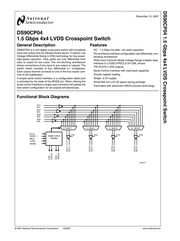
12. National Semiconductor 0590 04 December 12 2007 1 5 Gbps 4x4 LVDS Crosspoint Switch General Description 0 90 4 is a 4x4 digital cross point switch with broadside input and output pins for efficient board layout It utilizes Low Voltage Differential Swing LVDS technology for low power high speed operation Data paths are fully differential from input to output for low noise The non blocking architecture allows connections of any input to any output or outputs The switch matrix consists of four differential 4 1 multiplexes Each output channel connects to one of the four inputs com mon to all multiplexers A simple serial control interface or a configuration select port is activated by the state of the MODE pin When utilizing the serial control interface a single load command will update the new switch configuration for all outputs simultaneously Functional Block Diagrams Features DC 1 5 Gbps low jitter low skew operation Pin and Serial Interface configurable fully differential non blocking architecture Wide Input Common Mode Voltage Range enables easy interface to LI VDS LVPECL 2 5V CML drivers TRI STATE LVDS outputs Serial Control Interface with read back capability Double register loading Single 2 5V supply Small 6x6 mm LLP 32 space saving package Fabricated with advanced CMOS process technology IN1 Ni gt qt LL IN2 na 5 Tj IN3 att t
13. OUT3 OUT3 OUT2 OUT2 OUT1 OUT1 20028703 RSO RSCLK CSO CSCLK 20028702 Pin Descriptions Pin Name RN I O Type Description DIFFERENTIAL INPUTS COMMON TO ALL MUXES IN 1 4 Inverting and non inverting differential inputs IN1 15 IN2 Inverting and non inverting differential inputs 2 13 IN3 Inverting and non inverting differential inputs IN3 11 IN4 Inverting and non inverting differential inputs IN4 9 SWITCHED DIFFERENTIAL OUTPUTS OUT1 25 O LVDS Inverting and non inverting differential outputs OUT1 can be connected to any one pair OUT1 26 IN1 IN2 or IN4 OUT2 27 O LVDS Inverting and non inverting differential outputs OUT2 can be connected to any one pair OUT2 28 IN1 IN2 IN4 OUT3 29 O LVDS Inverting and non inverting differential outputs OUT3 can be connected to any one pair OUTS 30 1 IN2 IN3 or IN4 OUT4 31 O LVDS Inverting and non inverting differential outputs OUT4 can be connected to any one pair OUT4 32 IN2 IN4 DIGITAL CONTROL INTERFACE SCLK I LVCMOS Control clock to latch in programming data at Sl SCLK can be 0 MHz to 100 MHz SCLK should be burst of clock pulses active only while accessing the device After completion of programming SCLK should be kept at logic low to minimize potential noise injection into the high speed differential data paths SI SEL1 7 I LVCMOS Programming dat
14. T4 1 0 hRedundancy IN1 OUT1 OUT2 and IN3 OUT3 OUT4 Broadside IN1 OUT1 IN2 OUT2 IN3 OUTS IN4 OUT4 LH Low to High positive edge transition X Don t Care or Not Applicable lt a o www national com 4 IN1 IN1 IN2 IN2 IN3 IN3 IN4 IN4 IN1 IN1 IN3 IN3 SELO 1 SELO 0 SEL1 1 SEL1 0 OUT1 IN1 OUT1 IN1 OQUT2 OUT2 OUT3 OUT3 OUT4 OUT4 SELO 0 SELO 1 SEL1 1 0 OUT1 OUT1 OUT2 IN2 OUT2 IN2 OUT3 OUT3 OUT4 OUT4 FIGURE 1 DS90CP04 Configuration Select Decode OUT1 OUT1 OUT2 OUT2 OUT3 OUT3 OUT4 OUT4 OUT1 OUT1 OUT2 OUT2 OUT3 OUT3 OUT4 OUT4 20028704 www national com 0420650 0590 04 Absolute Maximum Ratings Note 1 If Military Aerospace specified devices are required Want please contact the National Semiconductor Sales Office LVDS Outputs 21 0 kV Distributors for availability and specifications LVDS Inputs 21 5 kV Supply Voltage Vpp 0 3V to 43V All Other Pins 24 0 kV Input Voltage 0 3V to 0 3V EIAJ O 200 pF 100V LVDS Receiver Input Voltage 0 3 to 3 3V LVDS Driver Output Voltage 0 3V to 3V Hecommended Operating LVDS Output Short Circuit Current 40mA Conditions Junction Temperature 150 C Min Typ Unit temperature 65 Cio 4150 C Supply Voltage GND 2375
15. a to select the switch configuration Data is latched into the input buffer register at the rising edge of SCLK SELO I LVCMOS Programming data to select the switch configuration CSO 18 O LVCMOS With MODE low control data is shifted out at CSO RSO for cascading to the next device RSO 2 in the serial chain The control data at CSO RSO is identical to that shifted in at SI with the exception of the device column row address being decremented by one internally before propagating to the next device in the chain CSO RSO is clocked out at the rising edge of SCLK CSCLK 19 O LVCMOS With MODE low these pins function as a buffered control clock from SCLK CSCLK RSCLK 3 RSCLK is used for cascading the serial control bus to the next device in the serial chain LOAD 22 LVCMOS When LOAD is high and SCLK makes a LH transition the device transfers the programming data in the load register into the configuration registers The new switch configuration for all outputs takes effect LOAD needs to remain high for only one SCLK cycle to complete the process holding LOAD high longer repeats the transfer to the configuration register MODE 23 I LVCMOS When MODE is low the SCLK is active and a buffered SCLK signal is present at the CLKOUT output When MODE is high the SCLK signal is uncoupled from register and state machine internals Internal registers will see an active low signal until MODE is brought Low again POWER 1 8 17 24 I
16. anteed to take place two clock cycles after programming has been completed Due to internal shift registers additional SCLK cycles will be necessary to complete array programming It takes 7 clock SCLK positive edge transitions for the control data to appear at RSO and CSO for its near neighbor Users must provide the correct number of clock transitions for the control data word to reach its destination in the array Table 3 shows an example of the control data words for a 4 device serial chain with connections OUT1 IN1 OUT2 IN2 OUT16 IN16 To program the array it requires four 30 bit control words to rip ple through the serial chain and reach their destinations In order to completely program the array in the 120 clock cycles associated with the 30 bit control words it is important to pro gram the last device in the chain first The following program ming data pushes the initial data through the chain into the correct devices Read Back Switch Configuration The DS90CP04 is put into read back mode by sending a spe cial Head start frame 01 1110 b Upon receipt of the special read start frame the configuration register information is trans ferred into the shift register and output at both RSO and CSO in the OUT1 to OUTA bit segments of the read control word Each time the read back data from a device passes through its downstream device its default address 11 1111 b is in ternally decremented by one The relative column add
17. are not production tested Note 3 Differential output voltage Vos is defined as OUT OUT I Differential input voltage Vp is defined as IIN IN I Note 4 Output offset voltage Vos is defined as the average of the LVDS single ended output voltages at logic high and logic low states Note 5 Characterized from any input to any one differential LVDS output running at the specified data rate and data pattern with all other 3 channels running K28 5 pattern at 1 25 Gb s asynchronously to the channel under test Jitter is not production tested but guaranteed through characterization on sample basis Random Jitter is measured peak to peak with a histogram including 1000 histogram window hits K28 5 pattern is repeating bit streams of 0011111010 1100000101 This deterministic jitter or DJ pattern is measured to a histogram mean with a sample size of 350 hits Like RJ the Total Jitter or TJ is measured peak to peak with a histogram including 3500 window hits 3 DC Source gt 100K IN M OUT RL 2 T VOUT wo Fe fu 05 dac i OUT RL 2 4 gt 100K VOS VOD VOUT VOUT 49 99 49 99 v Z vour gt 100K 20028712 FIGURE 2 Differential Driver DC Test Circuit www national com 8 OUT and OUT are connected to a ADVANTEST D3186 VDD 2 50 1000 differential transmission line Data Generator VID 250mV VOS 1 20V CSA8000 20028713 FIGURE 3 Differential Driver AC Test Circuit 500 950 resistor
18. e load register and all switches 2 are ready to be configured 13 www national com 0590 04 029 024 Row Address D23 D18 TABLE 4 A Read Back Example from a 4 Device Array Column Number of Address OUT1 OUT2 OUT3 OUT4 SCLK Descriptions D17 D12 D11 D9 D8 D6 D5 D3 D2 DO R C 20 3 R C 20 2 e fe gt ce fe e R C 0 1 Read Back R C 0 0 Note 7 LOAD and READ programming example is based on the 16x16 array configuration shown in Figure 11 Alternative expansion array configurations will require a slightly different programming sequence Switch Expansion For Minimum Programming Latency driven by the same load signal To prevent excessive stub Programming data ripples through the array through RSO and length in the array from affecting the signal quality of LOAD RSCLK in the row and CSO and CSCLK in the first column it is recommended that the load signal is distributed to each LOAD pins of all devices are electrically tied together and row or column in large crosspoint array applications www national com DEVICE 0 DEVICE 1 7 Clocks NUMBER OF SCLK POSITIVE EDGE TRANSITIONS 0 30 60 CONTROL WORD 1 01 F 1 0 1 E JEJE CONTROL WORD 1 01 F OM 2 2 4 4 01 F OO 91 F SFO 2 2 4 4 Device 1 Device O Configuration Ready to Configuration Ready Load to Load 20028707 FIGURE 11 14 Programming
19. iguration of the four channels of the device Table 1 and Table 2 are the bit defi nitions of the control word D29 is the first bit that shifts into Sl TABLE 1 30 Bit Control Word Descriptions The start frame for control word synchronization 01 1111 b LOAD Specify the row address of the device to be access The serial interface can access up to 64 devices in Specify the column address of the device to be access The serial interface can access up to 64 devices Specify the switch configuration for Output 1 See Table 2 Specify the switch configuration for Output 2 See Table 2 Specify the switch configuration for Output 3 See Table 2 Specify the switch configuration for Output 4 See Table 2 TABLE 2 Switch Configuration Data Bi D29 D24 E M D23 D18 the row 017 012 in the column MSB LSB OUT1 Connects to OUT2 sl Connects to OUT3 Connects to OUT4 Connects to Output 1 Tri Stated Output 2 Tri Stated Output 3 Tri Stated Output 4 Tri Stated MSB LSB OUT1 Connects to OUT2 Connects to OUT3 Connects to OUT4 Connects to 1 0 1 Invalid 1 1 0 Use of these invalid combinations may cause loss of synchronization 1 1 1 Row and Column Addressing The upper left device in an array of NxN devices is assigned row address O and column address O The devices to its right have column addresses of 1 to N whereas devices below it have row addresses of 1 to N The Serial Control In
20. ress emerges at RSO of the last device in the row and is used to determine 11 1111 b N the column of the sending device Similarly the row address emerges at CSO of the sending device After inserting the channel configuration information in the read control word the device will automatically revert to write mode ready to accept a new control word at SI Table 4 shows an example of reading back the configuration registers of 4 devices in the first row of a 4x4 device array Again due to internal shift registers additional SCLK cycles will be necessary to complete the array read It takes 4x30 SCLK clock cycles to shift out 4 30 bit configuration registers plus 7 SCLK cycles per device to account for device latency making for a total SCLK count of 148 The serialized read data is sampled at RSO and synchronized with RSCLK of the last device in the row The user is recommended to backfill with all O s at SI after the four reads have been shifted in TABLE 3 Example to Program a 4 Device Array Row Column Frame Address D29 D24 D23 D18 01 1111 01 1111 01 1111 01 1111 Control Word Destination Number of Address OUT1 OUT2 OUT3 OUT4 SCLK Device in Array D17 D12 D11 D9 D8 D6 D5 D3 D2 DO Cycles Row Column Shift in configuration information from device furthest from system SI input first to minimize array latency during the programming process 0420659 The 2 clock cycle delay ensures all channel information has reached th
21. rr INA gt 5 HHE TU 4 1 MUX1 SCLK gt I EN1 SI SEL1 Digital Control SELO Interface LOAD MODE gt gt OO x oo 9 OO mm 2007 National Semiconductor Corporation 200287 4 1 MUX2 EN2 4 M M OUT2 OUT2 4 1 MUX3 4 1 MUXA lt OUT3 OUT3 4 OUT4 20028701 www national com U21IMS 1010055019 SGA 5040 r0d206Sd 0590 04 SI SEL1 SELO SCLK MODE LOAD www national com INPUT ROW REGISTER DECREMENT E REGISTER COLUMN OUTPUT REGISTER COLUMN i DECREMENT CLOCK AND CONTROL LOAD SWITCH LL REGISTER pasas bum j r b m EN b um K j N ee ba eee J Co L DS90CP04 LLP 32 6x6x0 75mm body size 0 5mm pitch Top View Shown k admisit a tema F hmmm mm N e 1 ro hmmm w N I N I I N ep m I I I I I I N I Ww Kuwa I I Order Number DS90CP04TLQ DS90CP04TLQX Tape and Reel See NS Package Number LQA32A OUT4 OUT4
22. s provide a 20 1 attenuation network with CSA8000 Tek DG2020 Pulse Generator C is a lumped capacitance placed as close VOH VDD VDD 2 50V as possible to the device output VOL GND a a ss CSA8000 9500 500 Scope Termination MODE RSO EET m Es LOAD LOAD RSCLK SI SEL1 nee SI SEL1 Eon 7T HER LLLA seLo hH H seo CSCLK v V 1 DUT J C 15pF 1 VSS 0 0V Sidi Supe Termination Z Z 450 resistors provide a 10 1 mbh ambi darmi clle CS 20028714 FIGURE 4 LVCMOS Driver AC Test Circuit Note 6 9 www national com 0420650 0590 04 Note 6 The LVCMOS input and output AC specifications may also be verified and tested using an input attenuation network instead of a power splitter as shown in Figure 4 IN VOS 1 2V typical IN IN VID IN 20028715 FIGURE 5 LVDS Signals OUT OUT OUT VOD OUT 20028716 FIGURE 6 LVDS Output Transition Time IN IN SS SS SS eee c uer cce 0 0V OUT OUT DDV PESE sa m ai eae cs 20028717 FIGURE 7 LVDS Output Propagation Delay www national com 10 SCLK SI DSO RSO CSO RSCLK CSCLK tospir 20028718 FIGURE 8 Serial Interface Propagation Delay and Input Timing Waveforms SCLK MODE SCLK Internal DSCLK RSCLK CSCLK 20028719 FIGURE 9 Serial Interface MODE Timing and Functionalit
23. terface SCLK and SI is connected to the first device with the row and column addresses of 0 The Serial Control Interface shifts in a control word containing the row and column address of the device it wants to access When the control data propa gates through each device the control word s address is internally decremented by one before it is sent to the next row or column device When the control data is sent out the col umn interface CSO and CSCLK the row address is decre mented by one Similarly when the column address data is shifted out the row interface RSO and RSCLK the column address is decremented by one By the time the control word reaches the device it has been intended to program both the row and column addresses have been decremented to O Each device constantly checks for the receipt of a frame start 029 24 01 1111 b or 01 1110 b When it detects the proper start frame string and the row and column addresses it re ceives are both 0 the device responds by storing the switch configuration data of the 30 bit control word into its load reg ister Each device in the array is sequentially programmed through the serial interface When programming is completed for the entire array LOAD is pulsed high and the load register s con tent is transferred to the configuration register of each device The LOAD pulse must wait until the final bit of the control word has been placed into the load register This timing is guar
24. y 11 www national com 0420650 Load Configuration A LOAD or SELx OUT Configuration A Load Configuration B toy Configuration B 1 2V OUT f 50 90 20028720 FIGURE 10 Configuration and Output Enable Disable Timing Functional Descriptions PROGRAMMING WITH THE SERIAL INTERFACE The configuration of the internal multiplexer is programmed through a simple serial interface consisting of serial clock SCLK and serial input data line SI The serial interface is de signed for easy expansion to larger switch array A replicated output serial interface RSCLK RSO is provided for propa gating the control data to the downstream device in the row of an array of DS90CP04 devices in a matrix A similar repli cated serial interface CSCLK CSO is provided for propa gating the control data to the downstream devices in the first column of the device matrix Through this scheme user can program all the devices in the matrix through one serial control bus SCLK and SI with the use of the feed through replicated control bus at RSCLK and RSO CSCLK and CSO To program the configuration of the switch a 30 bit control word is sent to the device The first 6 bits shift the start frame into SI The only two valid start frames are 1F h for a config uration load and 1E h for a configuration read The start frame is followed by the row and column addresses of the device to be accessed as well as the switch conf
Download Pdf Manuals

Related Search