FAIRCHILD FQT4N25 250V N-Channel MOSFET Manual(1)
Contents
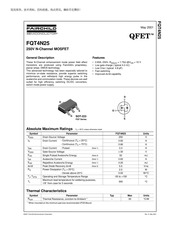
1. HABE RAGA GME Aman BAERS EE FAIRCHILD May 2001 Lp SEMICONDUCTOR QFET FQTAN25 250V N Channel MOSFET General Description Features These N Channel enhancement mode power field effect 0 83A 250V Rpston 1 750 AVgs 10 V transistors are produced using Fairchild s proprietary Low gate charge typical 4 3 nC planar stripe DMOS technology Low Crss typical 4 8 pF This advanced technology has been especially tailored to Fast switching minimize on state resistance provide superior switching Improved dv dt capability performance and withstand high energy pulse in the avalanche and commutation mode These devices are well suited for high efficiency switching DC DC converters switch mode power supply G SOT 223 FQT Series Absol ute Maxi mum Rati ngs Tg 25 C unless otherwise noted Symbol Parameter FQTAN25 Vpss Drain Source Voltage 250 Ip Drain Current Continuous Tc 25 C 0 83 Continuous Tc 70 C 0 66 lpm Drain Current Pulsed 3 3 Vess Gate Source Voltage 30 Single Pulsed Avalanche Energy 52 Avalanche Current 0 83 Repetitive Avalanche Energy 0 25 Peak Diode Recovery dv dt 5 5 Power Dissipation Tc 25 C 2 5 Derate above 25 C 0 02 Ty Tera Operating and Storage Temperature Range 55 to 4150 Maximum lead temperature for soldering purposes 1 8 from case for 5 seconds 300 T2. Thermal Characteristics Symbol Parameter Raja Thermal Resistance Junction to Ambient When mounted on the minimum pad size recommended PCB Mount 2001 Fairchild Semiconductor Corporation Rev A May 2001 GZNTLO4 Electrical Characteristics 1 250 unless otherwise noted Symbol Parameter Test Conditions Min Typ Max Units Off Characteristics BVpss Drain Source Breakdown Voltage Ves 0 V lp 250 uA 250 V ABVpss Breakdown Voltage Temperature Se lp 250 uA Referenced to 25 C vie ATy Coefficient p 8 be dis Joes Vps 250 V Veg 0 V 1 HA Zero Gate Voltage Drain Current Vps 200 V Tc 125 C 10 m lassr Gate Body Leakage Current Forward Vas 30 V Vps 0 V 100 nA lassR Gate Body Leakage Current Reverse Vas 30 V Vps 0 V 100 nA On Characteristics Vesith Gate Threshold Voltage Vps Vas lp 250 pA 3 0 5 0 Rps on Static Drain Source Vas 10 V Ip 0 415 A 1 7 Q On Resistance Ge R 1 38 S grs Forward Transconductance Vps 50V Ip 20 415 A Notes 1 28 E Dynamic Characteristics Ciss Input Capacitance Vps 25 V Veg 0 V 155 200 pF Coss Output Capacitance f 1 0 MHz 35 45 pF Css Reverse Transfer Capacitance 4 8 6 5 pF Switching Characteristics ta on Turn On
3. NEITHER DOES IT CONVEY ANY LICENSE UNDER ITS PATENT RIGHTS NOR THE RIGHTS OF OTHERS LIFE SUPPORT POLICY FAIRCHILD S PRODUCTS ARE NOT AUTHORIZED FOR USE AS CRITICAL COMPONENTS IN LIFE SUPPORT DEVICES OR SYSTEMS WITHOUT THE EXPRESS WRITTEN APPROVAL OF FAIRCHILD SEMICONDUCTOR CORPORATION As used herein 1 Life support devices or systems are devices or systems which a are intended for surgical implant into the body or b support or sustain life or c whose failure to perform when properly used in accordance with instructions for use provided in the labeling can be reasonably expected to result in significant injury to the user 2 A critical component is any component of a life support device or system whose failure to perform can be reasonably expected to cause the failure of the life support device or system or to affect its safety or effectiveness PRODUCT STATUS DEFINITIONS Definition of Terms Advance Information Formative or In This datasheet contains the design specifications for Design product development Specifications may change in any manner without notice Preliminary First Production This datasheet contains preliminary data and supplementary data will be published at a later date Fairchild Semiconductor reserves the right to make changes at any time without notice in order to improve design No Identification Needed Full Production This datasheet contains final specifications Fairchild Semiconductor r
4. T 2256 2 4 6 Ma Drain Source Voltage V Figure 5 Capacitance Characteristics E 10 5 3 3 Notes 2s Piso Tes 1 2 4 8 10 Vas Gate Source Voltage V Figure 2 Transfer Characteristics 7 7 E 10 o E E 150 C 25 C B 3X Notes 2 2 s Puse Test 107 1 L L 1 L 0 2 0 4 0 6 0 8 1 0 12 14 Vp Source Drain Voltage V Figure 4 Body Diode Forward Voltage Variation vs Source Current and Temperature 12 10r o 8f B gt et 8 8 8 2 gt 3X Note 3 6A e i i i i 0 1 2 3 4 5 Q Total Gate Charge nC Figure 6 Gate Charge Characteristics 92001 Fairchild Semiconductor Corporation Rev A May 2001 GeNVLOS Typical Characteristics continued Bur g EE ji 20 B N SA 5 15H eB Source B d Bos r 5 amp amp s nes a Beien 08 ji E L L L 0 0 L L i i 100 50 0 50 100 150 200 100 50 0 50 100 150 200 T Junction Temperature fg T Junction Temperature fg Figure 7 Breakdown Voltage Variation Figure 8 On Resistance Variation vs Temperature vs Temperature 10 LE EM ER at dE 08 T E lt F t 06 E Eu D 5 EMME o e E e i 8 E E E lt 2 X NES s 10 E 1 7 25 C 0 2 F 2T 15 C 3 Single Puise v as i i i i 10 1 10 1 25 50 75 100 125 150 Va Dra
5. 1 Package Dimensions SCcNU LOJ SOT 223 0 08MAX 3 00 0 10 Em iT i y m o e 0 06 1005 2 2 30 TYP p 0 70 0 10 NS L S 0 95 4 603025 0 95 0 25 0 05 gt a o m 0 65 0 20 1 75 0 20 3 50 0 20 7 00 0 30 r 60 S i 6 50 0 20 oo Mg 1 60 0 20 0 46 92001 Fairchild Semiconductor Corporation Rev A May 2001 TRADEMARKS The following are registered and unregistered trademarks Fairchild Semiconductor owns or is authorized to use and is not intended to be an exhaustive list of all such trademarks ACEx FAST OPTOPLANAR SuperSOT 3 Bottomless FASTr PACMAN SuperSOT 6 CoolFET FRFET POP SuperSOT 8 CROSSVOLT GlobalOptoisolator PowerTrench SyncFET DenseTrench GTO QFET TinyLogic DOME HiSeC Qs UHC EcoSPARK ISOPLANAR QT Optoelectronics UltraFET E CMOSTM LittleFE TTM Quiet Series VCX EnSigna MicroFET SLIENT SWITCHER FACT MICROWIRE SMART START FACT Quiet Series OPTOLOGIC Stealth DISCLAIMER FAIRCHILD SEMICONDUCTOR RESERVES THE RIGHT TO MAKE CHANGES WITHOUT FURTHER NOTICE TO ANY PRODUCTS HEREIN TO IMPROVE RELIABILITY FUNCTION OR DESIGN FAIRCHILD DOES NOT ASSUME ANY LIABILITY ARISING OUT OF THE APPLICATION OR USE OF ANY PRODUCT OR CIRCUIT DESCRIBED HEREIN
6. Delay Time Vpp 125 V Ip 3 6 A 6 8 25 ns ty Turn On Rise Time Ra 250 45 100 ns la oft Turn Off Delay Time 6 4 25 ns 4 Turn Off Fall Time Note 4 5 22 55 ns Qg Total Gate Charge Vps 200 V Ip 3 6 A 4 3 5 6 nC Qgs Gate Source Charge Ves 10 V 1 3 nC Ogg Gate Drain Charge Note 4 5 2 1 nC Drain Source Diode Characteristics and Maximum Ratings ls Maximum Continuous Drain Source Diode Forward Current 0 83 A Jeu Maximum Pulsed Drain Source Diode Forward Current 3 3 A Vsp Drain Source Diode Forward Voltage Vag 0 V 1g 0 83 A 1 5 V trr Reverse Recovery Time Vas 0 V Is 3 6 A zz 110 ns O Reverse Recovery Charge dle dt 100 A us Note 4 Se 0 35 uC Notes 1 Repetitive Rating Pulse width limited by maximum junction temperature 2 L 120mH las 0 83A Von 50V Rg 25 Starting Ty 25 C 3 Isp lt 3 6A di dt lt 300A us Von lt BVpss Starting Ty 25 C 4 Pulse Test Pulse width lt 300us Duty cycle lt 2 5 Essentially independent of operating temperature 2001 Fairchild Semiconductor Corporation Rev A May 2001 SeNVLOS Typical Characteristics lp Drain Current A 10 10 10 Ma Drain Source Voltage V Figure 1 On Region Characteristics lp Drain Current A Figure 3 On Resistance Variation vs Drain Current and Gate Voltage 8 c ES ad 6 cB 2 ba 3 Note
7. eserves the right to make changes at any time without notice in order to improve design Obsolete Not In Production This datasheet contains specifications on a product that has been discontinued by Fairchild semiconductor The datasheet is printed for reference information only 2001 Fairchild Semiconductor Corporation Rev H2
8. in Source Voltage V T Case Temperature C Figure 9 Maximum Safe Operating Area Figure 10 Maximum Drain Current vs Case Temperature Hu o E c LL o D 0 5 o X Notes z r Z Pul Pacto Dette 3 Ty To Pom Ze ell E d E Bo H TUT L 2 av R K I DZ pe M appe P NEHME 107 T k r r i aliii i rnb i aci iiud 4 iii 10 10 10 107 107 10 10 10 10 t Square Wave Pulse Duration sec Figure 11 Transient Thermal Response Curve 92001 Fairchild Semiconductor Corporation Rev A May 2001 SCcNr LOJ Gate Charge Test Circuit amp Waveform Same Type as DUT 12V gt Charge Resistive Switching Test Circuit amp Waveforms 90 10 Budou t on p t off Unclamped Inductive Switching Test Circuit amp Waveforms ar BVpss up Ue BVpss Voo BVpss las Ip t Vpp Vps t Let M Time 92001 Fairchild Semiconductor Corporation Rev A May 2001 SCcNU LOJ Vas Driver Isp DUT Peak Diode Recovery dv dt Test Circuit amp Waveforms Same Type as DUT e dv dt controlled by Re Isp controlled by pulse period Gate Pulse Width Gate Pulse Period lem Body Diode Forward Current di dt lam Body Diode Reverse Current Body Diode Recovery dv dt Von Body Diode Forward Voltage Drop GZNTLO4 2001 Fairchild Semiconductor Corporation Rev A May 200
Download Pdf Manuals

Related Search
FAIRCHILD FQT4N25 250V N Channel MOSFET Manual(1)