INFINEON BSP171P handbook
Contents
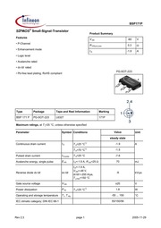
1. Infineon technologies BSP171P SIPMOS Small Signal Transistor Product Summary Features Vos P Channel R DS on max Enhancement mode Logic level Avalanche rated dv dt rated Pb free lead plating RoHS compliant PG SOT 223 2 4 Type Package Tape and Reel Information Marking 1 BSP 171P PG SOT 223 L6327 171P 3 Maximum ratings at T 25 C unless otherwise specified Parameter Symbol Conditions Value Unit steady state gt Continuous drain current T4595 C 1 9 1 o T2169 Pulsed drain current lopuise T a 25 C 7 6 Avalanche energy single pulse E as 15 1 9 A R gs725 Q 70 mJ lp 1 9 A Vps 48 V di dt 200 A us Tj max 150 C o lt is en t Reverse diode dv dt lt Gate source voltage Vos Power dissipation Operating and storage temperature 21 x lt T o cn a 150 IEC climatic category DIN IEC 68 1 55 150 56 Rev 2 3 page 1 2005 11 29 Infineon technologies BSP171P Parameter Symbol Conditions Thermal characteristics Thermal resistance junction soldering point Thermal resistance minimal footprint junction ambient steady state 6 cm cooling area Electrical characteristics at 7 25 C unless otherwise specified Static characteristics Drain source breakdown voltage Ves 0 V I p 250 HA co v Vos Ves Gate threshold vo2. gate 1 p 1 9A pulsed parameter T start parameter V pp 10 0 5 VBR DSS C 25 0 2 VBR DSS 0 8 VBR DSS lt gt 8 gt 0 1 1 10 100 1000 0 5 10 15 tay us Q gate nC 15 Drain source breakdown voltage 16 Gate charge waveforms Veross 7j p 1 mA 70 Vos 65 60 55 Veripss V 50 45 Q gate 40 Rev 2 3 page 7 2005 11 29 ne Infineon technologies BSP171P Package Outline SOT 223 Outline 6 5102 40 2 acc to DIN 6784 Footprint Packaging Tape C 5 0 4 Fide st H I Eld s 68 l1 1 75 Dimensions in mm Rev 2 3 page 8 2005 11 29 Infineon technologies BSP171P Published by Infineon Technologies AG Bereich Kommunikation St Martin StraBe 53 D 81541 M nchen Infineon Technologies AG 1999 All Rights Reserved Attention please The information herein is given to describe certain components and shall not be considered as warranted characteristics Terms of delivery and rights to technical change reserved We hereby disclaim any and all warranties including but not limited to warranties of non infringement regarding circuits descriptions and charts stated herein Infineon Technologies is an approved CECC manufacturer Information For further information on technology delivery terms and conditions and prices please contact your nearest Infineon Technologies office in Germany or our Infineon Technologies rep
3. ltage 57 460 pA 7 t It drai t V ps 60 V Ves 0 V ero gate voltage drain curren Tj 25 C V ps 60 V Ves 0 V Tj 125 C Gate source leakage current Drai tat ist Ves 4 5 V rain source on state resistance 1D 1 5A Ves 10 V 19 1 9 A IVbsl 2l DIR ps on max g7 1 5 A Transconductance Device on 40 mm x 40 mm x 1 5 mm epoxy PCB FR4 with 6 cm one layer 70 um thick copper area for drain connection PCB is vertical in still air Rev 2 3 page 2 2005 11 29 Infineon technologies Parameter Dynamic characteristics Input capacitance Output capacitance Reverse transfer capacitance Turn on delay time Rise time Turn off delay time Fall time Gate Charge Characteristics Gate to source charge Gate to drain charge Gate charge total Gate plateau voltage Output charge Reverse Diode Diode continuous forward current Diode pulse current Diode forward voltage Reverse recovery time Reverse recovery charge See figure 16 for gate charge parameter definition Rev 2 3 BSP171P V cs7 10 V 10 1 9 Re 6 Q V pp 48 V 1p 1 9 A V es 0 to 10 V Ves 0 V 1 9 A T 25 C VR 30 V I sl di dt 100 A us page 3 2005 11 29 e Infineon technologies BSP171P 1 Power dissipation 2 Drain current Piotr T Ip7f T 4 Vas 210 V 2 2 1 5 1 5 z T 1 4 a 7 0 5 0 5 0 0 0 40 80 120 160 0 40 80 120 160 TA C Ta C 3 Safe operating area 4 Max t
4. ransient thermal impedance Io f V ps T4925 C D 0 Z tnua f t p parameter t parameter D t T 10 10 lp A Zwus K W limited by on state resistance single pulse Vos IV Rev 2 3 page 4 2005 11 29 Infineon technologies BSP171P 5 Typ output characteristics 6 Typ drain source on resistance I p f V ps T 25 C R bS on p Tj 25 C parameter V os parameter V as 5 600 500 400 3 T E lt 5 a 300 i A 2 c 200 1 100 0 0 0 1 2 3 4 5 0 1 2 3 4 Vos V lp A 7 Typ transfer characteristics 8 Typ forward transconductance Ip7f V es IV psI 2l DIR psionmax 9 s f Ip Tj7 25 C parameter T 6 5 5 4 4 3 lt zy a 3 2 a 2 2 1 1 0 J 0 0 1 2 3 4 5 0 1 2 3 4 V cs V lp A Rev 2 3 page 5 2005 11 29 Infineon technologies 9 Drain source on state resistance R ps ony f T j p7 1 9 A Veg 10 V 500 400 98 R pS on MQ typ 100 11 Typ capacitances C z7f V 5s Ves 0 V f 1 MHz Rev 2 3 BSP171P 10 Typ gate threshold voltage V esth f T V es V ps p7 460 pA Vesqn V T C 12 Forward characteristics of reverse diode lE f V sp parameter T 10 25 C typ 150 C typ 10 Ir A 107 Vsp V page 6 2005 11 29 Infineon technologies BSP171P 13 Avalanche characteristics 14 Typ gate charge I Ag f t ay Res 25 Q Ves f Q
5. resentatives worldwide see address list Warnings Due to technical requirements components may contain dangerous substances For information on the types in question please contact your nearest Infineon Technologies office Infineon Technologies components may only be used in life support devices or systems with the expressed written approval of Infineon Technologies if a failure of such components can reasonably be expected to cause the failure of that life support device or system or to affect the safety or effectiveness of that device or system Life support devices or systems are intended to be implanted in the human body or to support and or maintain and sustain and or protect human life If they fail it is reasonable to assume that the health of the user or other persons may be endangered Rev 2 3 page 9 2005 11 29
Download Pdf Manuals

Related Search
INFINEON BSP171P handbook