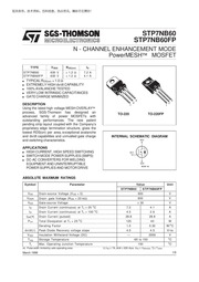
SGS-THOMSON STP7NB60 STP7NB60FP N - CHANNEL ENHANCEMENT MODE PowerMESH MOSFET handbook
Contents
1.2. Safe Operating Area for TO 220 Safe Operating Area for TO 220FP GC74840 GC74850 l0 A lo A 4 4 2 NUN 2 CN 10 c KIM N 10 ES SC E Sl 6 Ss 00 us 6 e 4 MV x 4 S tH 100 us ei E 2 5 NONI 2L a N o N H Ki 1ms 105 x 10 6 Oms B 4 4 10ms 2 2 i D C OPERATION E 10 10 6 6 4 4 D C OPERATION 2 2 2 2 10 a 4668 2 4 6B 27 46B 42 4 68 10 c 468 2 4 6B 2 3 458 10 10 10 10 Vos V 10 10 10 10 Vos V Zar 3 9 STP7NB60 FP Thermal Impedance for TO 220 SC20510 K 0 5 0 2 0 1 10 0 05 0 02 Zin K Ras A tp T m JUL SINGLE PULSE SL T 107 5 4 3 ap 1 10 10 10 o 107 tp s Output Characteristics GC74B50 GC74880 0 2 4 6 a bhlA 4 9 Thermal Impedance forTO 220FP GC20521 K 8 0 5 0 2 0 1 107 0 05
3. HAE RAGA BIER Aman BEREME kur SGS THOMSON STP7NB60 Yy MICROELECTRONICS STP7NB60FP N CHANNEL ENHANCEMENT MODE PowerMESH MOSFET TYPE Voss Rps on Ip STP7NB60 600 V 1 20 7 2 A STP7NB60FP 600 V 1 20 4 1 A TYPICAL Roson 1 0 Q EXTREMELY HIGH dv dt CAPABILITY 100 AVALANCHE TESTED VERY LOW INTRINSIC CAPACITANCES GATE CHARGE MINIMIZED DESCRIPTION Using the latest high voltage MESH OVERLAYTM process SGS Thomson has designed an TO 220 advanced family of power MOSFETs with outstanding performances The new patent pending strip layout coupled with the Company s proprietary edge termination structure gives the lowest RDS on per area exceptional avalanche and dv dt capabilities and unrivalled gate charge INTERNAL SCHEMATIC DIAGRAM and switching characteristics n APPLICATIONS a HIGH CURRENT HIGH SPEED SWITCHING sto a SWITCH MODE POWER SUPPLIES SMPS a DC AC CONVERTERS FOR WELDING EQUIPMENT AND UNINTERRUPTIBLE s POWER SUPPLIES AND MOTOR DRIVE SCOG 40 TO 220FP ABSOLUTE MAXIMUM RATINGS Symbol Parameter Unit TT rens Sene Vos Drain source Voltage Vos 0 60 V Drain gate Voltage Ras 20 kQ 60 Ly V Ip Drain Current continuous at Tc 25 C 7 2 4 1 A Ip Drain Current continuous at Tc 100 C 4 5 A Iom Drain Current pulsed 28 8 A Die Total Dissipation at Tc 25 C 125 W
4. 0 02 0 01 Zin K Rinu e KR auer PULSE h r JUL tpl E 10 107 10 107 107 10 4 s Transfer Characteristics 6074870 Io A 16 12 Vos 25V 8 4 0 6 12 18 24 Vos V Static Drain source On Resistance GC74890 Roston 9 1 4 0 8 Gate Charge vs Gate source Voltage GC74900 Vos V 10 0 10 20 30 40 50 Geint Normalized Gate Threshold Voltage vs Temperature GC74320 Vos th norm 1 1 1 0 0 9 0 8 0 7 0 6 50 0 50 100 1507 Source drain Diode Forward Characteristics 5C74940 Vsp V 1 1 T 40 C 25 C 0 9 150 C 0 7 0 5 0 3 o 4 8 12 16 Ispla 4 STP7NB60 FP Capacitance Variations GC74910 C pF 1600 1200 800 400 0 19 20 30 40 Vos DN Normalized On Resistance vs Temperature GC74930 Rostan norm 2 5 2 0 50 0 50 100 150 7 5 9 STP7NB60 FP Fig 1 Unclamped Inductive Load Test Circuit Fig 2 Unclamped Inductive Waveform UNCLAMPED INDUCTIVE WAVEFORMS VtBR DsS 5005870 Fig 3 Switching Time
5. Derating Factor 1 0 W C dv dt 1 Peak Diode Recovery voltage slope 4 5 4 5 V ns Viso insulation Withstand Voltage DG 200 V ic Tj Max Operating Junction Temperature 150 C e Pulse width limited by safe operating area 1 Isp lt 7A di dt lt 200 Aus Von lt Visa oss Tj Tumax March 1998 1 9 STP7NB60 FP THERMAL DATA 5 Rthj amb Thermal Resistance Junction ambient Max 62 C W Rthc sink Thermal Resistance Case sink Typ 0 5 C W Ti Maximum Lead Temperature For Soldering Purpose 300 C AVALANCHE CHARACTERISTICS Symbol Parameter Max Value Unit lar Avalanche Current Repetitive or Not Repetitive 72 A pulse width limited by T max lt 1 Single Pulse Avalanche Energy starting Tj 25 C Ip lan Voo 50 V OFF Parameter Test Conditions Drain source lIp 250u4A Vas 0 Breakdown Voltage Zero Gate Voltage Vos Max Rating Drain Current Vas 0 Vos Max Rating Te 125 C Gate body Leakage Vas 30V Current Vps 0 ON Vos Gate Threshold Voltage Vos Vas Io 250 uA Static Drain source On Vas 10V lp 3 6 A Resistance On State Drain Current Vos gt lp on X Rps on max Voss 10V DYNAMIC Parameter Test Conditions Min Typ Forward Vos gt lp on X Rps onymax Ip 3 6 A 4 5 3 Transconductance Ciss Input Capacitance Vps225V f 1MHz Ves 0 1250 1625 pF Coss Output Capacitance 165 223 pF Crss Reverse T
6. ransfer 16 22 pF Capacitance d 2 9 STP7NB60 FP ELECTRICAL CHARACTERISTICS continued SWITCHING ON Parameter Test Conditions Min Typ Max Turn on Time Vop 300 V Ip 3 6A 18 27 Rise Time Re 4 7 Q Vas 10V 12 see test circuit figure 3 Qg Total Gate Charge Vpop 480 V Io 7 2A Vas 10 V 30 45 nC Qgs Gate Source Charge 9 9 nC Qga Gate Drain Charge 13 3 nc SWITCHING OFF Parameter Test Conditions Off voltage Rise Time Vpp 480 V Ip 7 2A Fall Time Ra 4 70 Ves 10V Cross over Time see test circuit figure 5 Parameter Test Conditions Source drain Current Source drain Current pulsed Forward On Voltage Isp 7 2A Ves 0 Reverse Recovery Isp 7 2A di dt 100 A us Time Vop 100V Tj 150 C Reverse Recovery see test circuit figure 5 Charge Reverse Recovery Current Pulsed Pulse duration 300 us duty cycle 1 5 Pulse width limited by safe operating area
7. s Test Circuits For Resistive Load V 20V Vemax SC05930 Fig 5 Test Circuit For Inductive Load Switching And Diode Recovery Times 5005010 d 6 9 STP7NB60 FP TO 220 MECHANICAL DATA 4 7 9 STP7NB60 FP TO 220FP MECHANICAL DATA mm Q AB B oo D 8 9 d STP7NB60 FP Information furnished is believed to be accurate and reliable However SGS THOMSON Microelectronics assumes no responsability for the consequences of use of such information nor for any infringement of patents or other rights of third parties which may results from its use No license is granted by implication or otherwise under any patent or patent rights of SGS THOMSON Microelectronics Specifications mentioned in this publication are subjectto change without notice This publication supersedes and replaces all information previously supplied SGS THOMSON Microelectronics products are not authorized for use as critical components in life support devices or systems without express written approval of SGS THOMSON Microelectonics 1998 SGS THOMSON Microelectronics Printed in Italy All Rights Reserved SGS THOMSON Microelectronics GROUP OF COMPANIES Australia Brazil Canada China France Germany Italy Japan Korea Malaysia Malta Morocco The Netherlands Singapore Spain Sweden Switzerland Taiwan Thailand United Kingdom U S A Zar l 9 9
Download Pdf Manuals

Related Search
SGS THOMSON STP7NB60 STP7NB60FP N CHANNEL ENHANCEMENT MODE PowerMESH MOSFET handbook