ANALOG DEVICES AD1882 Manual
Contents
1. com 4 08 Rev 0 to Rev A Changed analog and digital power supply specifications 6 Changed analog and digital specifications and revised footnotes in Power Dowir States Derbi EPA CA Ut IPM 6 Rev Page 2 of 16 April 2008 GENERAL DESCRIPTION The AD1882 audio codec and SoundMAX software provides superior HD audio quality that exceeds Vista Premium perfor AD1882 Table 2 Typical Desktop Configuration with 5 1 on 3 Jacks mance The AD1882 has six DACs and four ADCs two stereo Port Function headphone ports C LFE swapping digital and analog PCBeep PortA Front Panel Headphone and S PDIF output making the AD1882 the right choice for Port B Front Panel Microphone desktop PCs where performance is the primary consideration Port C Rear Panel Line In Surround The jack retasking feature on this product supports various con Port D Rear Panel Line Out Headphone figurations including platforms for 5 1 on 5 or 3 jacks and front Port E Rear Panel Microphone C LFE panel jack retasking The AD1882 is available in a 48 lead RoHS compliant lead Table 3 Typical Notebook Configuration frame chip scale package in both reels and trays See Ordering Port Function Guide on Page 16 Port A Headphone ADDITIONAL INFORMATION a hile bate Port C Internal Microphone This data sheet provides a general overview of the AD1882 Port D Internal Stereo Speakers SoundMAX codec s2. 24 2E 30 3C 24 00000027 26 00002105 27 00002105 29 00002104 2A 00002106 2C 00002131 2D 0000001E 2F 00171514 17 37 00000403 39 00000014 3A 00000015 3C 00000017 Rev A 14 of 16 April 2008 In Table 12 default configuration values are set on codec power up only Default configuration values are not reset by link or soft reset to preserve modifications by BIOS control Table 12 Default Configuration Bytes AD1882 31 30 29 28 27 24 23 20 19 16 15 12 8 7 4 3 0 Location Misc JD Over Name Value Connectivity Chasis Position Def Device Conn Type Color Ride Def Assn Sequence Port A Headphone 0221401F Jack External Front HP Out 1 8 Jack Green 0 1 F Port D Front L R 01014010 Jack External Rear Line Out 1 8 Jack Green 0 1 0 Mono Out 901701 0 Fixed Internal N A Speaker Other Analog Unknown 1 F 0 Port B Front Mic 02A190FO Jack External Front Mic In 1 8 Jack Pink 0 F 0 Port C Line In 01813021 Jack External Rear Line In 1 8 Jack Blue 0 2 1 Port Surr Back 01011012 Jack External Rear Line Out 1 8 Jack Black 0 1 2 Port Rear Mic 01A19020 Jack External Rear Mic In 1 8 Jack Pink 0 2 0 CD IN 9933012E Fixed Internal Special 3 CD ATAPI Unknown 1 2 E Analog PCBeep 90F701FO0 Internal N A Other Other Analog Unknown 1 F 0 S PDIF Out 014511 0 Jack External Rear SPDIF Out Optical Black 1 F 0 Port G C LFE 01016011 Jack E
3. A Mixer 2 Audio Mixer Mixes the Port A selected DAC and mixer output amps to drive Port A 23 VREF Power Down F Vendor Defined Powers down the internal and external VREF circuitry 24 Port G C LFE 4 Pin Complex Rear panel C LFE jack 26 Port E Mixer 2 Audio Mixer Mixes DAC_1 and mixer output amps to drive Port E 27 Port G Mixer 2 Audio Mixer Mixes DAC_1 and mixer output amps to drive Port G 29 Port D Mixer 2 Audio Mixer Mixes DAC 0 and mixer output amps to drive Port D 2A Port F Mixer 2 Audio Mixer Mixes DAC 2 and mixer output amps to drive Port F 2C Port C Mixer 2 Audio Mixer Mixes the Port C selected DAC and mixer output amps to drive Port C 2D Stereo Mix Down 2 Audio Mixer Mixes the stereo L R channels to drive mono output 2F BIAS Power Down F Vendor Defined Powers down the internal MIC BIAS FILT and all MIC BIAS pins 37 Port A Out Selector 3 Audio Selector Selects the Port A DAC 0 1 39 Port B Boost 3 Audio Selector Microphone boost amp for Port B 3A Port C Boost 3 Audio Selector Microphone boost amp for Port C 3C Port E Boost 3 Audio Selector Microphone boost amp for Port E Rev A 11 of 16 April 2008 AD1882 HD AUDIO PARAMETERS The SSID value is set on codec power up only SSID is not reset by link or soft reset in order to preserve modifications by BIOS control Table 8 Root and Function Node Parameters Sub Func Group Audio Vendor ID Revisio
4. dB Fundamental 80 dB ADC VOLUMES Step Size ADCSEL 0 ADCSEL 1 1 5 dB PGA Gain Attenuation Range 58 5 22 5 dB Mute Attenuation of 0 dB Fundamental 80 dB ANALOG MIXER Signal to Noise Ratio SNR Input to Output 95 dB CD to Port D Output 95 dB Port B C or E to Port D Output 95 dB Port A to Port D Output 95 dB Port D to Port A Output 95 dB Step Size All Mixer Inputs 1 5 dB Input Gain Attenuation Range All Mixer Inputs 34 5 12 0 dB ANALOG LINE LEVEL OUTPUTS Full Scale Output Voltage 1 0 1 0 Vrms Ports C t Vp p 1 X kQ Output Capacitance 15 pF External Load Capacitance 1000 pF ANALOG HP DRIVE OUTPUTS Full Scale Output Voltage 1 0 V rms Ports Aand D 2 83 V p p Output Impedance 0 5 Q External Load Impedance 32 Q Output Capacitance 15 pF External Load Capacitance 1000 pF ANALOG INPUTS CD Port D When Used as Input 1 Vrms 2 83 Vp p Microphone Boost Amplifier Ports B C or E Boost 0 dB 1 Vrms When Used as Inputs 2 83 V p p Boost 10 dB 0 316 V rms 0 894 V p p Boost 20 dB 0 1 V rms 0 283 V p p Boost 30 dB 0 032 Vrms 0 089 Vp p Input Impedance 20 Input Capacitance 5 7 5 pF Rev A 5 of 16 April 2008 AD1882 Table 4 AD1882 General Specifications Continued Parameter Min Typ Max Unit Digital GPIO Pins GPIO 0 GPIO_1 EAPD Input Signal High Vi x 0 60 V Input Signal Low Vi 0 DVio x 0 24 V
5. 0000009 80000000 13 0040050C 00010010 00000001 00000009 80051F1F 14 00400081 00003727 00000000 15 0040018D 00003737 00000001 80000000 16 0040018D 00000017 00000001 80000000 17 0040098D 00003737 00000001 80000000 18 00400001 00000020 00000000 19 00500500 00000002 00000009 1A 00400000 00000020 00000000 1B 0 00 0 0 1D 000000 0000 1E 2 3 8 1F 00 00100 00000010 00000001 20 0020010 80051517 00000008 21 00300100 00000001 80051F1F 22 00200103 80000000 00000002 23 00F00100 00000008 24 0040098D 00000017 00000001 80000000 26 00200103 80000000 00000002 27 00200103 80000000 00000002 29 00200103 80000000 00000002 2A 00200103 80000000 00000002 2C 00200103 80000000 00000002 2D 00200100 00000001 2F 00 00100 00000003 37 00300101 00000002 39 00300100 00000001 00270300 00300100 00000001 00270300 3C 0030010D 00000001 00270300 Rev A 13 of 16 April 2008 AD1882 Table 11 Connection List Node ID Connections 0 2 0 3 4 7 NID NID NID NID NID NID NID NID 02 0000001D 1D 03 04 05 08 0000000C 0C 09 0000000D OD OB 00000908 08 09 18BC3911 20123B3B 11 39 1 3C 18 3B 3B 12 20 00 18BC3911 20123B3B 11 39 1 3C 18 3B 3B 12 20 10 11 00000022 22 12 00000029 29 13 0000002D 2D 14 15 0000002C 2C 16 0000002A 2A 17 00000026 26 18 19 00002120 20 21 1A 1B 00000002 1D 00000B01 1E 00002104 1F 000000 A 21 00000020 22 00002137 23 2209811 BC30AE24 20 22
6. ANALOG DEVICES High Definition Audio SoundMAX Codec AD1882 FEATURES 2 stereo headphone amplifiers Microsoft Vista Premium logo for notebook and desktop 95 dB audio outputs 90 dB audio inputs Internal 32 bit arithmetic for greater accuracy Impedance and presence detection on all jack pins Digital synthesis PCBeep C LFE channel swapping 2 general purpose digital I O GPIO pins Advanced power management modes EAPD control for internal speakers 48 lead Pb free LFCSP_VQ package SIX 96 kHz DACs 3 independent stereo DAC pairs Independent 8 kHz 11 025 kHz 16 kHz 22 05 kHz 32 kHz 44 1 kHz 48 kHz 88 2 kHz and 96 kHz sample rates 16 20 and 24 bit PCM resolution Selectable stereo mixer on outputs ww FOUR 96 kHz ADCs 2 independent stereo ADC pairs Simultaneous record of up to 4 channels Independent 8 kHz 11 025 kHz 16 kHz 22 05 kHz 32 kHz 44 1 kHz 48 kHz 88 2 kHz and 96 kHz sample rates 16 20 and 24 bit resolution S PDIF OUTPUT Supports 44 1 kHz 48 kHz 88 2 kHz and 96 kHz sample rates 16 20 and 24 bit data widths PCM and AC3 formats Digital PCM gain control DEDICATED AUXILIARY PINS Stereo CD input w GND sense Mono out pin for internal speakers or telephony Analog PCBeep input pin DIGITAL AD1882 BEEP PORTF PORT D gt PORTG OUT L E
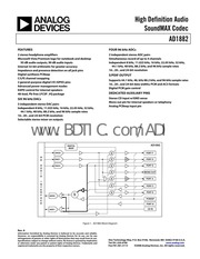
7. CC VIZ VY 1 T E R F A LA A A Figure 1 AD1882 Block Diagram Rev A Information furnished by Analog Devices is believed to be accurate and reliable However no responsibility is assumed by Analog Devices for its use nor for any infringements of patents or other rights of third parties that may result from its use Specifications subject to change without notice No license is granted by implication or otherwise under any patent or patent rights of Analog Devices Trademarks and registered trademarks are the property of their respective owners One Technology Way P O Box 9106 Norwood MA 02062 9106 U S A Tel 781 329 4700 www analog com Fax 781 461 3113 2008 Analog Devices Inc All rights reserved AD1882 TABLE OF CONTENTS Fe 1 o 2 Cereral DESPON 3 Additional Informatio 3 Tack Gone T Cii tT m 3 4 Wi DEN UIT E E 4 General Specifications 4 HD Audio Link Specifications 6 Power Down States 6 Absolute Maximum Ratings 7 7 Environmental Conditions i reor ree trenes y Pin Configuration and Function Descriptions 8 HD Anda OD deme 11 HD Audio Parameters 12 Gulias DIMENSIONS esi nr p RS DM 16
8. Input Leakage Current Signal High 150 nA Input Leakage Current Signal Low li 50 Output Signal High lour 500 x 0 72 V Output Signal Low lour 1500 0 DVio 0 10 S PDIF_OUT Output Signal High lour 500 0 72 Output Signal Low lour 1500 uA 0 0 10 V Power Supply Analog AV 3 3 V 5 Power Supply Range 3 13 3 30 3 46 V Power Dissipation 116 mW Supply Current 35 mA Digital DVpp 3 3 V 10 Power Supply Range 2 97 3 30 3 63 V Power Dissipation 162 mW Supply Current 49 mA Digital 3 3 V 1096 Power Supply Range 2 97 3 30 3 63 V Power Dissipation 3 96 mW Supply Current 1 20 mA Power Supply Rejection 100 mV Signal 1 kHz 80 dB Guaranteed but notte BI Measurements AAWAY C RMS values assume HD AUDIO LINK SPECIFICATIONS HD Audio signals comply with the High Definition Audio spec ifications Please refer to these specifications at www intel com standards hdaudio POWER DOWN STATES Table 5 Power Down States Parameter IDypp Typ lAypp Typ Unit Function Node In DO All Nodes Active 49 35 mA Function Node in D3 16 0 7 mA Codec in RESET 3 3 mA Individual block power savings DAC Pair Powered Down Saves Each 6 6 mA ADC Pair Powered Down Saves Each 5 44 mA Mixer Power Control and Associated Amps Saves 0 3 mA MIC BIAS Powered Down Saves 0 1 0 mA Powering down the BIAS p
9. T A R 41 LI MIC HP LO Front Panel Headphone Line Out PORT G L 43 LO SWAP Rear Panel C LFE Output PORT G R 44 LO SWAP Rear Panel C LFE Output FILTER REFERENCE MIC BIAS B 28 Switchable Microphone Bias For use with Port Pins 21 22 MIC_BIAS C 29 Switchable Microphone Bias For use with Port Pins 23 24 MIC_BIAS E 31 Switchable Microphone Bias For use with Port E Pins 14 15 DV core 1 CAUTION DO NOT APPLY 3 3 V TO THIS PIN Filter connection for internal core voltage regulator This pin must be connected to filter caps 10 uF 1 0 uF and 0 1 uF connected in parallel between Pin 1 DVs Pin 4 VREF_FLT 27 Voltage Reference Filter This must be connected to filter caps 1 0 uF and O 1uF connected in parallel between Pin 27 and AVs Pins 26 42 The symbols used in this table are defined as Input O Output LI driving headphone load MIC Line level input LO Line level output HP Output capable of Input supports microphones with MIC bias and boost amplifier SWAP Outputs can swap L R channels typically used to support C LFE or shared C LFE function Rev A Page9 of 16 April 2008 01882 Table 6 AD1882 Pin Descriptions Continued Mnemonic Pin Function Description POWER AND GROUND DV jo 3 3V 3 Connect to the I O Voltage Used for the HD Audio Controller Signals DVss 4 7 Digital Supply Return Ground DVpp 3 3 V 9 Digi
10. architecture and functionality Additional Port E Docking Station Line In Microphone information on the AD 1882 is available in the AD1882 Pro grammers Reference Manual Please contact your local Analog Devices Inc sales representative for more information For information on SoundMAX codecs and software see Analog Devices website at www analog com soundMAX JACK CONFIGURATION used when selecting por Table 1 T k Port Function Port A Front Panel Headphone Port B Front Panel Microphone Port C Rear Panel Line In Port D Rear Panel Line Out Headphone Port E Rear Panel Microphone Port F Rear Panel Surround Port G Rear Panel C LFE Rev A Page3 of 16 April 2008 AD1882 SPECIFICATIONS TEST CONDITIONS Parameter Test Condition Temperature 25 C Digital Supply 3 3V Analog Supply 3 3V MIC BIAS IN via Low Pass Filter 5 0V Sample Rate f 48 kHz Input Signal Frequency Sine Wave 1008 Hz Amplitude for THD 3 0 dB Full Scale Analog Output Pass Band 20 Hz to 20 kHz DAC 10 Output Load Line Out Tests 32 Output Load Headphone Tests ADC 0 dB Gain PERFORMANCE Parameter Min Typ Max Unit Line Out Drive 10 Loads DAC to Pin Total Harmonic Distortion THD 85 dB Dynamic Range 60 dB in Ref to amp A Weighted 95 dB Signal to Noise Ratio 95 dB Headphone Drive 32 O Loads DAC to Pin Total Harmonic Distortion THD 83 dB Dyna
11. erters 05 DAC 2 0 Audio Output Stereo C LFE channel digital audio converters 08 ADC 0 1 Audio Input Stereo record channel 1 audio digital converters 09 ADC 1 1 Audio Input Stereo record channel 2 audio digital converters 0B S PDIF Mix Selector 3 Audio Selector Selects which ADC drives the S PDIF mixer oC ADC Selector 0 3 Audio Selector Selects and amplifies attenuates the input to ADC 0 00 ADC Selector 1 3 Audio Selector Selects and amplifies attenuates the input to ADC_1 10 Digital Beep 7 Beep Generator Internal digital PCBeep signal 11 Port A Headphone 4 Pin Complex Front panel headphone microphone jack 12 Port D Front L R 4 Pin Complex Rear panel front headphone jack 13 Mono Out 4 Pin Complex Monorail output pin internal speakers or telephony system 14 Port B Front Mic 4 Pin Complex Front panel microphone headphone jack 15 Port C Line In 4 Pin Complex Rear panel line in jack 16 Port F Surr Back 4 Rear panel surround rear 5 1 jack 17 Port E Rear Mic 4 panel mic jack 18 D 4 Analog CD i 1 E 1A 4 1 S PDIF Out 4 Pin Complex S PDIF output pin 1D S PDIF Mixer 2 Audio Mixer Mixes the selected ADC with the digital stream to drive S PDIF out 1E Mono Out Mixer 2 Audio Mixer Selects which source drives the mono out signal 20 Analog Mixer 2 Audio Mixer Mixes individually gainable analog inputs 21 Mixer Output Atten 3 Audio Selector Attenuates the mixer output to drive the Port mixers 22 Port
12. eset DIGITAL GPIO 0 2 General Purpose Input Output Pin Digital signal used to control external circuitry GPIO_1 EAPD 47 1 0 General Purpose Input Output Pin EAPD Pin Digital signal used to control external circuitry Defaults to high Z When used as EAPD high Z amp on DVss amp off SPDIF_OUT 48 S PDIF_OUT Supports S PDIF output JACK SENSE AND EAPD SENSE_A SRC_B 13 JACK SENSE A D Input Sense Drive SENSE_B SRC_A 34 JACK SENSE Input Sense A Drive ANALOG PCBEEP 12 LI Monaural Input from System for Analog PCBeep PORT E_L 14 LI MIC LO SWAP Auxiliary Input Output Left Channel PORT E_R 15 MIC LO SWAP Auxiliary Input Output Right Channel PORT F_L 16 1 0 Auxiliary Input Output Left Channel PORT F_R 17 Auxiliary Input Output Right Channel CD_L 18 LI CD Audio Left Channel CD_GND 19 LI CD Audio Analog Ground Reference for Differential CD Input Must be connected to AGND via 0 1 mF capacitor if not in use as GND CD 20 LI D Audi hannel PORT B L LI MiG Front Panel Stereo M E 0 LI MIC Front Pa M E 0 1 LI Rear Panel Stereo MIC Line In PORT C_R 24 LI MIC LO Rear Panel Stereo MIC Line In PORT D L 35 LI HP LO Rear Panel Headphone Line Out PORT D R 36 LI HP LO Rear Panel Headphone Line Out PORT A L 39 LI MIC HP LO Front Panel Headphone Line Out MONO OUT 40 LO Monaural Output to Internal Speaker or Telephony Subsystem Speakerphone POR
13. mic Range 60 dB in Ref to f A Wei 95 dB Signal to Nois amp R dB Input Ports Pin dB Total Harmonic Di 81 dB Dynamic Range 60 dB in Ref to f A Weighted 90 dB Signal to Noise Ratio 90 dB GENERAL SPECIFICATIONS Table 4 AD1882 General Specifications Parameter Min Typ Max Unit DIGITAL DECIMATION AND INTERPOLATION FILTERS f 8 kHz to 192 Pass Band 0 0 4 f Hz Pass Band Ripple 0 005 dB Stop Band 0 6 fs Hz Stop Band Rejection dB Group Delay 20 100 1 6 Group Delay Variation Over Pass Band 0 us ANALOG TO DIGITAL CONVERTERS Resolution 24 Bits Gain Error Full Scale Span Relative to Nominal Input Voltage 10 Interchannel Gain Mismatch Difference of Gain Errors 0 5 dB ADC Offset Error 5 ADC Crosstalk Line Inputs Input L Ground R Read R Input R Ground L Read L 85 Line Inputs to Other 100 80 dB Rev A Page 4 of 16 April 2008 AD1882 Table 4 AD1882 General Specifications Continued Parameter Min Typ Max Unit DIGITAL TO ANALOG CONVERTERS Resolution 24 Bits Gain Error Full Scale Span Relative to Nominal Input Voltage 10 Interchannel Gain Mismatch Difference of Gain Errors 0 5 dB Total Audible Out of Band Energy Measured from 0 6 x f to 100 kHz 85 dB DAC Crosstalk Input L Zero Read R_OUT Input Zero L Read L_OUT 95 dB DAC VOLUMES Step Size DAC 0 DAC 1 DAC 2 1 5 dB Output Gain Attenuation Range 58 5 0 dB Mute Attenuation of 0
14. n ID Count Type Caps GPIO Caps NodelD 00 01 02 03 04 05 08 11 00 ROOT 0x11D4 1882 0x0010 0300 0x0001 0001 01 FUNCTION 0x0002 003 0x0000 0001 0x0001 OCOC 0 4000 0002 Subject to change with silicon stepping Table 9 Subsystem ID 31 16 15 8 7 0 Node ID Name Type Value SSID SKU ASM ID 0x01 FUNCTION Function OxBFD2 0000 OxBFD2 0x00 0x00 The default SSID is over written by platform BIOS after power on It is preserved across HD Audio link reset and verb reset ww BDT conf Rev A Page 12 of 16 April 2008 Table 10 Widget Parameters AD1882 Output Volume Widget Stream Pin Input Amp ConnList Processing Amp Knob Capabilities PCM Size Formats Capabilities Capabilities Length States Caps Capabilities Capabilities NodelD 09 0 0 oc OE OF 10 12 13 01 00000480 000E01FF 00000001 80000000 00000009 00052727 02 00030310 000 01 0 00000005 00000001 80052727 03 00000405 000E01FF 00000001 00000000 00000009 00052727 04 00000405 000E01FF 00000001 00000000 00000009 00052727 05 00000405 000E01FF 00000001 00000000 00000009 00052727 08 00100501 000E01FF 00000001 00000001 00000009 09 00100501 000E01FF 00000001 00000001 00000009 OB 00300301 00000002 0C 0030010D 00000008 80053627 00 00300100 00000008 80053627 10 0070000C 00000000 800BOFOF 11 0040018D 0000373F 00000001 80000000 12 0040058D 0001003F 00000001 0
15. owers down all port BIAS pins This disables all microphone bias circuits set to 10096 or 50 setting them to the high Z state The 0 Q and high Z states remain unaffected by the BIAS power state Rev A Page6 of 16 April 2008 ABSOLUTE MAXIMUM RATINGS Stresses greater than those listed below may cause permanent damage to the device This is a stress rating only functional operation of the device at these or any other conditions above those indicated in the operational section of this specification is not implied Exposure to absolute maximum rating conditions for extended periods may affect device reliability ENVIRONMENTAL CONDITIONS Ambient Temperature Rating Tams Tease PD x Oca Tease case temperature in C PD power dissipation in W Oca thermal resistance case to ambient Oja thermal resistance junction to ambient thermal resistance junction to case AD1882 Power Supplies Rating All measurements per EIA JESD51 with 252 test board per Digital DVpp 0 30 V to 3 65 V EIA JESD51 7 Digital 1 0 0 30 V to 3 65 V Analog AVpp 0 30 V to 3 65 V Pack Unit Input Current Except Supply Pins 10 0 mA E Osa Oca E Analog Input Voltage Signal Pins 0 30 V to AVpp 0 3 V LFCSP VO ar 15 32 c w Digital Input Voltage Signal Pins 0 30 V to DVio 0 3 V Ambient Temperature Operating 0 C to 70 C Storage Temperat
16. tal Supply Voltage 3 3 This is regulated down to DVcoge on Pin 1 to supply the internal digital core internal to the AD1882 AVpp 3 3 V 25 38 CAUTION DO NOT APPLY 5 0 TO THESE PINS Analog supply voltage 3 3 V ONLY Note AVpp supplies should be well regulated and filtered as supply noise degrades audio performance MIC_BIAS_IN 33 Source Power for Microphone Bias Boost Circuitry AVss 26 42 Analog Supply Return Ground should be connected to DV using a conductive trace under or close to the AD1882 The symbols used in this table are defined as Input O Output LI Line level input LO Line level output HP Output capable of driving headphone load MIC Input supports microphones with MIC bias and boost amplifier SWAP Outputs can swap L R channels typically used to support C LFE or shared C LFE function ww C com Rev A Page10 of16 April 2008 HD AUDIO WIDGETS In the following table node IDs that are not shown are reserved for future use Table 7 HD Audio Widgets AD1882 Node ID Type ID Type Description 00 ROOT x Root Device identification 01 FUNCTION x Function Designates this device as an audio codec 02 S PDIF DAC 0 Audio Output S PDIF digital stream output interface 03 DAC 0 0 Audio Output Headphone surround side 7 1 channel digital audio converters 04 DAC 1 0 Audio Output Stereo front channel digital audio conv
17. ure 65 C to 150 C ESD CAUTION ESD electrostatic discharge sensitive device Charged devices and circuit boards can discharge without detection Although this product features patented or proprietary protection circuitry damage may occur on devices subjected to high energy ESD Therefore proper ESD precautions should be taken to Rev A Page7 of 16 April 2008 avoid performance BUT AU 401882 PIN CONFIGURATION AND FUNCTION DESCRIPTIONS RESERVED NC GPIO_1 EAPD RESERVED NC RESERVED NC MONO_OUT gt a A PORT G_R PORT G_L PORT A_L PORT D_R PORT D_L DVio SENSE B SRC A DVss MIC BIAS IN SDATA OUT RESERVED NC AD1882JCPZ BIT CLK MIC BIAS E TOP VIEW RESERVED NC Not To Scale DVpp MIC_BIAS B PORT E_R PORT B_R PORT C_R T E SENSE_A SRC_B Figure 2 AD1882 48 Lead Package and Pinout Rev A Page8 of 16 April 2008 Table 6 AD1882 Pin Descriptions AD1882 Mnemonic Pin No Function Description DIGITAL INTERFACE SDATA_OUT 5 Link Serial Data Output AD1882 input stream Clocked both edges of the BIT_CLK BIT_CLK 6 Link Bit Clock 24 000 MHz serial data clock SDATA_IN 8 1 0 Link Serial Data Input AD1882 output stream Clocked only on one edge of BIT_CLK SYNC 10 Link Frame Sync RESET 11 Link Reset AD1882 master hardware r
18. xternal Rear Line Out 1 8 Jack Orange 0 1 1 ww C comi Rev A 15 of 16 April 2008 AD1882 OUTLINE DIMENSIONS Dimensions are shown in millimeters 0 30 1 EE 0 60 MAX 0 18 EXPOSED 5 25 PAD BOTTOM VIEW ix So 0 50 0 40 pap 0 25 MIN f 100 42 MAX 022 BS 0 50 BSC COPLANARITY SEATING 0 20REF 0 08 PLANE COMPLIANT TO JEDEC STANDARDS MO 220 VKKD 2 Figure 3 48 Lead Lead Frame Chip Scale Package LFCSP_VQ Body V Quad P 48 own illimeters ORDERING GUIDE Model Temperature Range Package Description Package Option AD1882JCPZ 0 C to 70 C 48 Lead LFCSP_VQ CP 48 1 AD1882JCPZ RL 0 to 70 C 48 Lead LFCSP VQ 13 Tape and Reel CP 48 1 17 RoHS Compliant Part 2008 Analog Devices Inc All rights reserved Trademarks and AN ALOG registered trademarks are the property of their respective owners www analo g com uum La DEVICES Rev A Page16 of16 April 2008
Download Pdf Manuals

Related Search
ANALOG DEVICES AD1882 Manual history of analog devices analog.com ad8043 analog devices adc tutorial analog devices application notes analog devices home page analog devices p/n ad8479 ad8232 set up function analog discovery 2 ad2 analog devices inc. adi