ANALOG DEVICES ADM222/ADM232A/ADM242* handbook
Contents
1. OUTPUTS INPUTS 2ouT R2in OUT ADM232A EN GND INTERNAL 400kO PULL UP RESISTOR 16 INTERNAL 400kO PULL UP RESISTOR ON EACH TTL CMOS INPUT ON EACH TTL CMOS INPUT INTERNAL 5kO PULL DOWN RESISTOR INTERNAL 5kO PULL DOWN RESISTOR ON EACH RS 232 INPUT ON EACH RS 232 INPUT Figure 10 ADM232A Typical Operating Circuit Figure 12 ADM242 Typical Operating Circuit REV A ADM222 ADM232VADM242 Typical Performance Characteristics 15 15 10 10 gt 5 1 5 lt 1 0 d o gt o gt gt o 5 x 5 V Tx O P LO 10 10 15 15 5 10 15 20 25 30 0 2 4 6 8 10 12 14 LOAD CURRENT mA LOAD CURRENT mA TPC 1 Charge Pump V V vs Current TPC 4 Transmitter Output Voltage vs Current 9 115kBps 230kBps 115kBps 3 RE TUR Secon TRANSMITTER OUTPUT VOLTAGE V 460kBps 1 5 460 7 230kBps a 0 500 1000 1500 2000 2500 3000 LOAD CAPACITANCE pF TPC 2 Transmitter Baud Rate vs Load Capacitance TPC 5 Charge Pump V V Exiting Shutdown z i A 6 0V T A 600ns 2 9V l 1 1 1 1 1 1 i CH1 10 0V 5 00V Mi 00us CH2 64V CH1 10 0V 5 00 Mi 00us CH2 64V TPC 3 Transmitter Unloaded Slew Rate TPC 6 Transmitter Fully Loaded S2. Driver Inputs These inputs accept TTL CMOS levels An internal 400 kQ pull up resistor to Vcc is connected on each input Tour Transmitter Driver Outputs These are RS 232 levels typically 9 V Rw Receiver Inputs These inputs accept RS 232 signal levels An internal 5 pull down resistor to GND is connected on each of these inputs Rout Receiver Outputs These are TTL CMOS levels NC No Gomnect No are required to this pig EN ADM242 Only Active Low Digital Input May be used to enable or disable three state both receiver outputs SHDN ADM222 and ADM242 Active Low Digital Input May be used to disable the device so that the power consumption is minimized On the ADM222 all drivers and receivers are disabled On the ADM242 the drivers are disabled but the receivers remain enabled NC NO CONNECT Figure 8 ADM222 DIP and SOIC Pin Configurations REV ADM222 ADM232A ADM242 TOP VIEW 5 Not to Scale Figure 9 ADM232A DIP SOIC Pin Configuration Figure 11 ADM242 DIP SOIC Pin Configuration 5V INPUT 5V INPUT 0 1pF Vee 0 1pF 5V TO 10V c1 5V TO 10V 0 1pF a VOLTAGE DOUBLER 0 14 F ci VOLTAGE DOUBLER C2 45V TO 10V 45V TO 10V VOLTAGE INVERTER V C2 VOLTAGE INVERTER V 0 1uF Ti Tlout Tin TTL CMOS RS 232 TTL CMOS RS 232 INPUTS OUTPUTS INPUTS OUTPUTS T2iN 2 2IN Riour TTL CMOS RS 232 TT CMOS RS 232 OUTPUTS INPUTS
3. Option ADM222AN 40 to 85 C Plastic DIP N 18 ADM222AR 40 to 85 Wide SOIC R 18W ADM232AAN 40 to 85 C Plastic DIP N 16 ADM232AARN 40 C to 85 C Narrow SOIC R 16N ADM232AARW 40 to 85 Wide SOIC R 16W ADM242AN 40 to 85 Plastic DIP N 18 ADM242AR 40 to 85 Wide SOIC R 18W NAL Vin ov Vout RECEIVER OUTPUT VoL 0 5V VoL Figure 4 Receiver Disable Timing ADM222 ADM232A ADM242 TRANSMITTER SHDN INPUT ov OUTPUT V Figure 6 Transmitter Shutdown Disable Timing INPUTS TTL CMOS OUTPUTS R2 C1 5V TO 10V ci VOLTAGE DOUBLER vx C2 45V TO 10V C2 VOLTAGE INVERTER V OUT 16 INTERNAL 400 PULL UP RESISTOR ON EACH TTL CMOS INPUT INTERNAL 5 PULL DOWN RESISTOR ON EACH RS 232 INPUT Figure 7 ADM222 Typical Operating Circuit PIN FUNCTION DESCRIPTION Mnemonic Function Power Supply Input 5 V 10 V Internally generated positive supply 10 V nominal V Internally generated negative supply 10 V nominal GND Ground Pin Must be connected to 0 V 1 External capacitor 1 terminal is connected to this pin External capacitor 1 terminal is connected to this pin C2 External capacitor 2 terminal is connected to this pin C2 External capacitor 2 terminal is connected to this pin Transmitter
4. 16 Lead Plastic DIP N 16 0 840 21 34 0 745 18 92 PN 0 280 7 11 0 240 6 10 PIN 14 0 060 1 52 0 015 0 38 MAX LARA RA RA 0 130 0 160 4 06 3 30 0 115 2 93 be NMIN 0 022 0 558 0 100 0 070 1 77 SEATING 0 014 0 356 2 54 0 045 1 15 16 Lead Wide SOIC R 16W 0 4133 10 50 0 3977 10 00 16 9 0 2992 7 60 0 2914 7 40 0 41935 10 65 1 8 1 Ss ta ped 0 PINT 4 950 1 27 0 1043 2 65 BSC 0 0926 2 35 X 4 gt lt 0 0118 0 30 0 0192 0 49 SEATING 0 0040 0 10 0 0138 0 35 PLANE 040125 0 42 0 0091 0 23 0 210 5 33 0 015 0 38 MAX yA 0 130 0 160 4 06 l E 3 30 0 115 2 93 ig oe MIN R 16N 0 3937 10 00 0 3859 9 80 A 0 1574 4 00 19 91 0 2440 6 20 0 325 8 25 0 1497 3 80 0 284 5 80 0 300 7 62 __ ITF bod oo 0 195 4 95 PIN 0 050 1 27 0 0688 1 75 0 115 2 93 BSC 0 0532 1 35 0 015 0 381 0 008 0 204 0 0098 0 25 0 0192 0 49 SEATING 8 0 OUTLINE DIMENSIONS Dimensions shown in inches and mm 16 Lead Narrow SOIC 0 0040 0 10 0 0138 0 35 PLANE 0 0075 0 19 0 0196 0 50 0 0099 0 25 45 Y ra 0 0099 0 25 0 0 0500 1 27 0 0160 0 41 18 Lead Wide SOIC R 18W 0 4
5. 625 11 75 0 4469 11 35 18 10 0 2992 7 60 1 0 2914 7 40 0 4198 10 65 1 9 9 0 3937 10 00 0 0291 0 74 PIN 1 0 1043 2 65 0 0291 0 74 45 HAIDE ID AF pidm x 45 0 0098 0 25 0 0926 2 35 0 0098 0 25 X 4 gt ie gt 8 gt 0 0500 1 27 0 0118 0 30 0 0500 0 0192 0 49 SEATING 0 0 0500 1 27 0 0157 0 40 30040070 1 27 0 0138 0 35 PLANE 0 0125 0 32 USt 0 10 j 0 0091 0 23 0 0157 0 40 18 Lead Plastic DIP N 18 0 925 23 49 4 0 845 21 47 0 280 7 11 0 240 6 10 0 325 8 25 PIN 17 paced 0 060 1 52 0 200 7 62 0 195 4 95 3 0 115 2 93 0 015 0 381 0 008 0 204 0 022 0 558 0 100 0 070 1 77 SEATING 0 014 0 356 cal 0 045 1 15 REV 01213 0 1 01 rev PRINTED IN U S A
6. ANALOG DEVICES High Speed 5 V 0 1 pF CMOS RS 232 Drivers Receivers ADM222 ADM232A ADM242 FEATURES 200 kB s Transmission Rate Small 0 1 uF Charge Pump Capacitors Single 5 V Power Supply Meets All EIA 232 E and V 28 Specifications Two Drivers and Two Receivers On Board DC DC Converters 9 V Output Swing with 5 V Supply 30 V Receiver Input Levels Pin Compatible with MAX222 MAX232A MAX242 APPLICATIONS Computers Peripherals Modems Printers Instruments GENERAL DESCRIPTION The ADM222 ADM232A ADM242 are a family of high speed RS 232 line drivers receivers offering transmission rates up to 200 kB s Operating from single 5 V power Supply a highly efficient on chip charge pumpjusidsg small OLUF external capacitors allows RS 232 bipolar Tevel to besdeveloped Two RS 232 drivers and two RS 232 receivers are provided on each device The devices are fabricated on BiCMOS an advanced mixed technology process that combines low power CMOS with high speed bipolar circuitry This allows for transmission rates up to 200 kB s yet minimizes the quiescent power supply current to under 5 mA The ADM222A is a pin compatible high speed upgrade for the AD232 and for the ADM232L It is available in 16 lead DIP and in both narrow and wide surface mount SOIC packages The ADM222 contains an additional shutdown SHDN func tion that may be used to disable the device thereby reducing the supply current to 0 1
7. C W Power Dissipation R 16N 400 mW Derate 7 mW C above 70 C Oja Thermal Impedance 80 C W Power Dissipation R 16W 400 mW Derate 7 mW C above 70 C 0j Thermal Impedance 80 CW Power Dissipation 18 400 mW Derate 7 mW C above 70 C 0j Thermal Impedance 80 C W Test Circuits Vin teur V Vout ov V Figure 1 Transmitter Propagation Delay Timing EN INPUT ter 3 5V 0 8V RECEIVER OUTPUT Figure 2 Receiver Enable Timing INN D REV A Power Dissipation R 18W 400 mW Derate 7 mW C above 70 C Oja Thermal Impedance 80 C W Operating Temperature Range Industrial A Version 40 C to 85 C Storage Temperature Range 65 to 150 C Lead Temperature Soldering 10 sec 300 C Vapor Phase 60 sec 215 C Infrared 15 sec ob PR dr wig ee 220 C This is a stress rating only and functional operation of the device at these or any other conditions above those indicated in the operation sections of this specifica tion is not implied Exposure to absolute maximum rating conditions for extended periods of time may affect reliability ORDERING GUIDE Temperature Package Package Model Range Description
8. e Web Site http www analog com Fax 781 326 8703 Analog Devices Inc 2001 ADM222 ADM232A ADM242 SPECIFICATION Vec 5 V 10 C1 64 0 1 pF all spec ifications Tm 10 Tmax unless otherwise noted Parameter Typ Max Unit Test Conditions Comments RS 232 TRANSMITTERS Output Voltage Swing 5 9 V Transmitter Outputs Loaded with to Ground Input Logic Threshold Low 1 7 0 8 V Tin Input Logic Threshold High 2 4 1 7 V Logic Pull Up Current 12 40 uA Tw 0V Data Rate 200 kB s Output Resistance 300 Q Vee V V 0 V Vout 2 V Output Short Circuit Current Instantaneous 10 mA RS 232 RECEIVERS RS 232 Input Voltage Range 30 30 V RS 232 Input Threshold Low 0 8 1 2 V RS 232 Input Threshold High 1 6 2 4 V RS 232 Input Hysteresis 0 2 0 4 1 0 V 5 RS 232 Input Resistance 3 5 7 kQ Ta 0 C to 85 TTL CMOS Output Voltage Low VoL 0 05 0 4 V lour 3 2 mA TTL CMOS Output Voltage High 3 5 V Iour 1 0 mA TTL CMOS Output Short Circuit Current 2 85 Source Current GND TTL CMOS Output Short Circuit Current 10 35 mA Sink Current TTL CMOS Output Leakage Current 0 05 10 uA SHDN GND EN Vec 0 lt Vour lt EN Input Threshold Low Vp 1 4 0 8 V EN Input Threshold High 2 0 1 4 V POWER SUPPLY Power Supply Current 4 8 mA No Load 13 mA 3 Load on Both Outputs Shutdown Power Supply Curren
9. lew Rate 6 REV ADM222 ADM232A ADM242 GENERAL INFORMATION The ADM222 ADM232A ADM242 are high speed RS 232 drivers receivers requiring a single digital 5 V supply The RS 232 standard requires transmitters that will deliver 5 V minimum on the transmission channel and receivers that can accept signal levels down to 3 V The parts achieve this by integrating step up voltage converters and level shifting transmitters and receivers onto the same chip CMOS technology is used to keep the power dissipation to an absolute minimum All devices con tain an internal charge pump voltage doubler and a voltage inverter that generates 10 V from the 5 V input Four exter nal 0 1 uF capacitors are required for the internal charge pump voltage converter The ADM222 ADM232A ADM242 is a modification enhance ment and improvement to the AD230 AD241 family and derivatives thereof It is essentially plug in compatible and does not have materially different applications CIRCUIT DESCRIPTION The internal circuitry consists of four main sections These are Charge Pump Voltage Converter TTL CMOS to RS 232 Transmitters RS 232 to TTL CMOS Receivers Enable and Shutdown Functions Charge Pump DC DC Voltage Converter The Charge Pump Voltage converter consists of an oscillator and a switching matrix The converter generates a 10 V supply from the input 5 V level This is done in tworstagessusing a switched capacitor technique The 9 stip
10. ply is doubled to 10 V using capacitor 1 5 charg storage element The 10 V level is also generated from the input 5 V supply using C1 and C2 as the storage elements Capacitors C3 and C4 are used to reduce the output ripple Their values are not critical and can be reduced if higher levels of ripple are acceptable The charge pump capacitors and C2 may also be reduced at the expense of higher output imped ance on the and V supplies The V and V supplies may also be used to power external circuitry if the current requirements are small Please refer to the typical performance characteristics which shows the V V output voltage vs current In the shutdown mode the charge pump is disabled and V decays to Vcc while V decays to 0 V Transmitter Driver Section The Drivers convert TTL CMOS input levels into RS 232 output levels With Vcc 5 V and driving a typical RS 232 load the output voltage swing is 9 V Even under worst case conditions the drivers are guaranteed to meet the 5 V RS 232 minimum requirement REV A The input threshold levels are both TTL and CMOS compat ible with the switching threshold set at Vcc 4 With a nominal 5 V the switching threshold is 1 25 V typical Unused inputs may be left unconnected as an internal 400 kO pull up resistor pulls them high forcing the outputs into a low state As required by the RS 232 standard the slew rate is limited to less than 30 V us
11. t 9 1 10 uA SHDN Input Leakage Current i i 1 SHDN Input Threshold Low VNE 1 4 0 8 SHDN Input Threshold High 2 0 1 4 V AC CHARACTERISTICS Transition Region Slew Rate 3 8 30 V us C 50 pF to 1000 pF Ry 3 to 7 Measured from 3 V to 3 V or 3 V to 3 V Transmitter Propagation Delay TTL to RS 232 0 85 3 5 us 1 0 3 5 Us tpLHT Receiver Propagation Delay RS 232 to TTL 0 1 0 5 us tPHLR Receiver Output Enable Time 125 500 ns TER Receiver Output Disable Time 160 500 ns tpr Transmitter Output Enable Time 250 us SHDN Goes High Transmitter Output Disable Time 3 5 us SHDN Goes Low Transmitter to Propagation Delay Difference 150 ns Receiver to Propagation Delay Difference 200 ns Guaranteed by design not production tested Specifications subject to change without notice 2 REV A ADM222 ADM232A ADM242 ABSOLUTE MAXIMUM RATINGS T4 25 C unless otherwise noted VG 6V 0 3 V to 13 V Nee ot 0 3 V to 13 V Input Voltages Tin cT 0 3 V to Vcc 0 3 V RN Gua ere eae 30 V Output Voltages TOUT ak hae i aaa A V 0 3 V to V 0 3 V Ropi ue ded 0 3 V to Vcc 0 3 V Short Circuit Duration FOU Terima s SO ead ROLE Continuous Power Dissipation 16 400 mW Derate 7 5 mW C above 70 C Oja Thermal Impedance 80
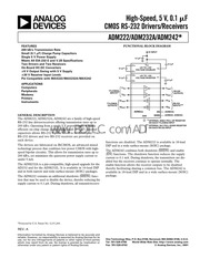
12. uA During shutdown all transmit receive Protected by U S Patent No 5 237 209 REV A Information furnished by Analog Devices is believed to be accurate and reliable However no responsibility is assumed by Analog Devices for its use nor for any infringements of patents or other rights of third parties which may result from its use No license is granted by implication or otherwise under any patent or patent rights of Analog Devices FUNCTIONAL BLOCK DIAGRAM 0 5V TO 10V VOLTAGE DOUBLER 5V TO 10V VOLTAGE INVERTER V 0 0 1pF Tin TTL CMOS INPUTS 2 Riour TTL CMOS OUTPUTS R2out ADM2xx ADM242 ADM222 ADM242 INTERNAL 400kO PULL UP RESISTOR ON EACH TTL CMOS INPUT INTERNAL 5 PULL DOWN RESISTOR ON EACH RS 232 INPUT functions are disabled The ADM222 is available in 18 lead DIP and in a wide surface mount SOIC package The ADM242 combines both shutdown SHDN and enable EN functions The shutdown function reduces the supply current to 0 1 mA During shutdown the transmitters are dis abled but the receivers continue to operate normally The enable function allows the receiver outputs to be disabled thereby facilitating sharing a common bus The ADM242 is available in 18 lead DIP and in a wide surface mount SOIC package One Technology Way P O Box 9106 Norwood MA 02062 9106 U S A Tel 781 329 4700 World Wid
13. without the need for an external slew limiting capacitor and the output impedance in the power off state is greater than 300 Receiver Section The receivers are inverting level shifters that accept RS 232 input levels 3 V to 15 V and translate them into 5 V TTL CMOS levels The inputs have internal 5 pull down resistors to ground and are also protected against overvoltages of up to 30 V The guaranteed switching thresholds are 0 8 V mini mum and 2 4 V maximum which are well within the 3 V RS 232 requirement The low level threshold is deliberately positive as it ensures that an unconnected input will be inter preted as a low level The receivers have Schmitt trigger input with a hysteresis level of 0 5 V This ensures error free reception for both noisy inputs and for inputs with slow transition times Enable and Shutdown Functions On the ADM222 both receivers are fully disabled during shutdown On the ADM242 both receivers continue to operate normally This function is useful for monitoring activity so that when it ocotirs ean be takenfjout of the shutdown mode TheADM242 enable function EN which can be used to fully disable the receivers independent of SHDN APPLICATIONS INFORMATION A selection of typical operating circuits is shown in TPCs 1 6 and Figure 13 Figure 13 Transmitter Output Disable Timing ADM222 ADM232A ADM242
Download Pdf Manuals

Related Search
ANALOG DEVICES ADM222/ADM232A/ADM242* handbook