TOREX XC74WL4066SR Manual
Contents
1. INPUT O O OUTPUT Input by sine wave ViN 0dBm f 1MHz 8 11 XC74WL4066SR FEED THROUGH TEST CIRCUIT O 0 1 uF fin O OUTPUT RIN 502 6002 O Vcc 2 Input by sine wave ViN 0dBm f 1MHz CROSS TALK CONTROL INPUT gt SWITCH OUTPUT Test Circuit Pulse Generator Vin O O OUTPUT Vcc 2 e Waveform Vcc fCONT 1MHz duty cycle 50 INPUT tr tf 3ns GND TOIREX 9 11 XC74WL4066SR I CROSS TALK BETWEEN SWITCHES Test Circuit fin OUTPUT1 50Q VcoNT VIL Vcc 2 INPUT RL 6002 fin O OUTPUT2 50pF Vec 2 Waveform fiN 1MHz INPUT tr tf 3ns 10 11 XC74WL4066SR The products and product specifications contained herein are subject to change without notice to improve performance characteristics Consult us or our representatives before use to confirm that the information in this datasheet is up to date We assume no responsibility for any infringement of patents patent rights or other rights arising from the use of any information and circuitry in this datasheet Please ensure suitable shipping controls including fail safe designs and aging protection are in force for equipment employing products listed in this datasheet The products in this datasheet are not developed designed or approved for use with such equipment whose failure of malfunc2. 1 0 HA Power On Leak Current Is ON 5 5 VIN Vcc oR GND _ 0 1 1 0 HA Control Input Current ICONT 0 5 5 Vin Vcc or GND _ x 0 1 1 0 u A Static Supply Current Icc 5 5 or GND _ _ 2 0 _ 20 0 HA 2 11 XC74WL4066SR SWITCHING ELECTRICAL CHARACTERISTICS tr tf 3ns Ta 25 C Ta 40 C 85 C PARAMETER SYMBOL CONDITIONS 2 UNITS CL Vcc V MIN TYP MAX MIN MAX 2 0 x 2 5 12 0 15 0 15pF 3 3 _ 2 0 4 0 _ 5 5 ns 5 0 Delay Time tPHL 2 0 4 0 20 0 23 0 50pF 3 3 9 0 6 0 8 0 ns 5 0 2 0 5 0 6 0 2 0 8 5 45 0 60 0 15pF 3 3 4 5 9 0 11 0 ns tzL 5 0 3 5 7 5 _ 9 0 Output Enable Time tzH 2 0 9 0 50 0 65 0 50pF 3 3 E 5 0 10 0 m 12 0 ns 5 0 4 0 8 5 10 0 2 0 9 0 45 0 55 0 15pF 3 3 e 7 0 17 0 20 0 ns 12 5 0 6 0 14 0 18 0 Output Disable Time tHZ 2 0 12 0 60 0 _ 75 0 50pF 3 3 10 0 23 0 27 0 ns 5 0 8 0 20 0 25 0 RL 10kO Sine Wave Distortion Rate 50pF 3 0 0 05 E fiN 1kHz RL 6000 Band Width 50pF 3 0 Vout 200 20log10 3dB VIN Feed Through 50pF 3 0 RL26000 60 dB Switch off 2 0 R 600Q T 60 2 z b 50pF 3 0 1 100
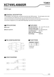
3. TOIREX XC74WL4066SR CMOS Logic GENERAL DESCRIPTION XC74WL4066SR is dual analog switch manufactured using silicon gate CMOS processes The small supply current which is one of the features of the CMOS logic gives way to high speed operations which enables LS TTL With wave forming buffers connected internally stabilized output can be achieved as the series offers high noise immunity As the series is integrated into a mini molded MSOP 8B package high density mounting is possible H APPLICATIONS e Palmtops Digital equipment EPIN CONFIGURATION 1 ay 8 Vcc on 2 7 CONT coNT2 3 4 6 on2 GND 4 d Vo 2 MSOP 8B TOP VIEW m LOGIC DIAGRAM VO 1 CONT2 5o o 2 FEATURES High Speed Operations tod 1 5ns TYP Vcc 5V Operating Voltage Range 2V 5 5V Low Power Consumption 2u A MAX Ta 25 C Low ON Resistance 120 TYP CMOS Logic Dual Analog Switch Small Package MSOP 8B m FUNCTIONS CONTROL STATE L OFF H ON H High level L Low level 1 11 XC74WL4066SR mm ABSOLUTE MAXIMUM RATINGS Ta 40 C 85 C PARAMETER SYMBOL RATINGS UNITS Supply Voltage Vcc 0 5 6 0 V Input Voltage VCONT 0 5 6 0 V Output Voltage Vi o 0 5 Vcc 0 5 V Input Diode Current 20 Output Diode Current IOK 20 Swi
4. mV n Control Switches 4 5 150 2 0 _ 60 Cross Talk 5OpF 30 RL 26000 60 dB Between Switches P d fin 1 MHz 4 5 60 Control Input Capacitance 5 10 10 pF Switch Input Output Capacitance CiN ouT 6 Feed Through Capacitance CIN OUT 0 5 Power Dissipation Capacitance Cpd 13 pF TOIREX 3 11 XC74WL4066SR MON RESISTANCE Test Circuit O O INPUT O O OUTPUT d VIN OUT Ron Q 103 VIN OUT Input Voltage Dependancies of ON Resistance RON RONmax RON 1 VIN vec 4 11 XC74WL4066SR m POWER OFF LEAK CURRENT Vcc VCONT VIL m POWER ON LEAK CURRENT Vcc TOIREX 5 11 XC74WL4066SR E DELAY TIME Test Circuit O Pulse Generator O OUTPUT RIN 502 CL Waveform Vcc INPUT tr tf 3ns GND OUTPUT VoL 6 11 XC74WL4066SR BOUTPUT ENABLE TIME OUTPUT DISABLE TIME Test Circuit OUTPUT I Waveform Vcc fCONT 1MHz NDOT tr tf 3ns GND OUTPUT VoL VOH OUTPUT VoL TOIREX 7 11 XC74WL4066SR ESINE WAVE DISTORTION RATE O O OUTPUT Input by sine wave W 3dB BAND WIDTH
5. tch Output Current lio 25 Voc GND Current ICC IGND 50 Power Dissipation 25 300 mW Storage Temperature Range Tstg 65 150 C Note Voltage is all ground standardized RECOMMENDED OPERATING CONDITIONS PARAMETER SYMBOL CONDITIONS UNITS Supply Voltage Vcc 2 5 5 V Input Voltage VCONT 075 5 V Output Voltage Vi o 0 VCC V Operating Temperature Range Topr 40 85 C 0 200 VCC 3 3V Input Rise and Fall Time tr tf ns 0 100 VCC 5V mDC ELECTRICAL CHARACTERISTICS Ta 25 C Ta 40 C 85 C PARAMETER SYMBOL CONDITIONS r UNITS Vcc V MIN TYP MAX MIN MAX 2 0 1 50 1 50 _ High Level ViH 3 0 2 10 2 10 V Control Input Voltage 5 5 3 85 3 85 _ 2 0 _ 0 50 B 0 50 Low Level VIL 3 0 0 90 B 0 90 V Control Input Voltage 5 5 1 65 1 65 2 0 VconT VIH B 130 350 550 Peak ON Resistance RoNmax 3 0 Vin 0 Vcc 22 50 65 4 5 IiIN OUT 1mA 12 25 35 2 0 23 50 65 ON Resistance RoN 1 3 0 ViN GND or Vcc 14 90 40 4 5 IiN OUT 1mA 10 20 25 2 0 13 35 55 Switch ON Resistance A RON 3 0 Vin 0 Vcc _ 3 6 _ 8 Differential 4 5 liN OUT 1mA 2 4 6 Power Off Leak Current Is OFF 5 5 VconT VIL Vin Vcc VouT GND 0 1 x
6. tion can be reasonably expected to directly endanger the life of or cause significant injury to the user e g Atomic energy aerospace transport combustion and associated safety equipment thereof Please use the products listed in this datasheet within the specified ranges Should you wish to use the products under conditions exceeding the specifications please consult us or our representatives We assume no responsibility for damage or loss due to abnormal use All rights reserved No part of this datasheet may be copied or reproduced without the prior permission of TOREX SEMICONDUCTOR LTD TOREX SEMICONDUCTOR LTD TOIREX 11 11
Download Pdf Manuals

Related Search
TOREX XC74WL4066SR Manual